
|
|
Forum Index : Microcontroller and PC projects : Another Pico Backpack
| Page 1 of 2 |
|||||
| Author | Message | ||||
| panky Guru Joined: 02/10/2012 Location: AustraliaPosts: 1094 |
Like others, I decided to build a Backpack for my Pico using what modules and components I had at hand. It is using an ILI9341 2.8" LCD, an RTC module and can take either an HC-12 Wireless module or an ESP8266-01 WiFi module. All the I/O pins are brought out to 0.1" pitch connectors grouped for function (SPI, I2C, Serial, analogue but can be configured for almost anything. I used connectors available from Jaycar here in Australia but you could use any 0.1" pitch connector. For the power, I have it so you can use USB 5V and the Pico's 3.3V, Ext 5V and the Pico's 3.3V or Ext 5V and backpack 3.3V configurable by jumpers. The Pico, HC-12 oe ESP modules mount on top of the board and the LCD on the back. It is an 85mm x 85mm board with the board and lcd sharing mounting holes. I designed the board using Diptrace and would be happy to supply the Diptrace PCB to anyone who wants it. Note that the 3D functionality will be limited to the board only as I have designed quite a number of the 3D component images myself. The PCB is currently being manufactured by LDElectronics here in Australia - more expensive than overseas but I do like supporting local if I can. Some pics: 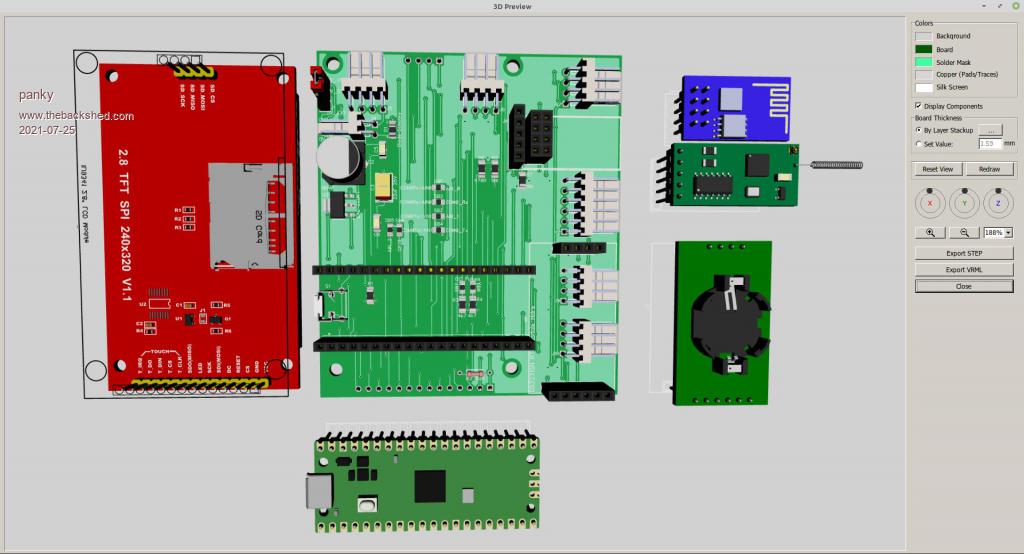 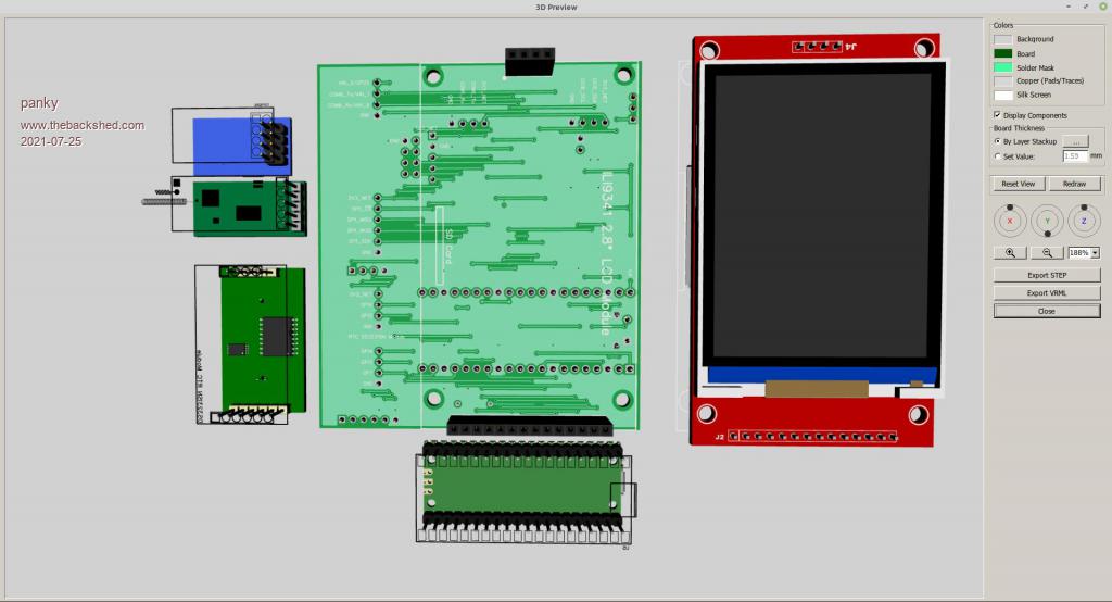 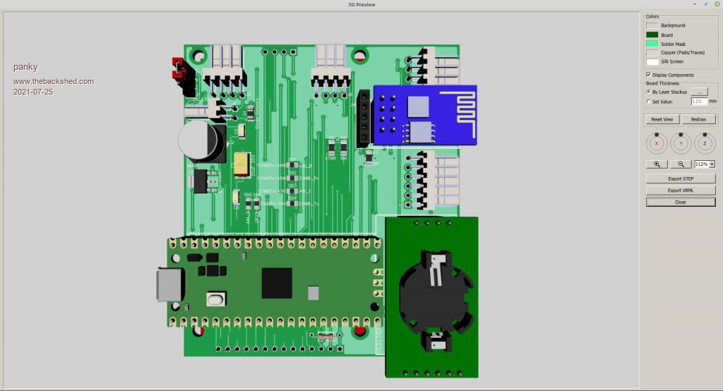 ... almost all of the Maximites, the MicromMites, the MM Extremes, the ArmMites, the PicoMite and loving it! |
||||
palcal Guru Joined: 12/10/2011 Location: AustraliaPosts: 1798 |
I would like to try a local manufacturer, the extra cost may be offset by less postage. What did they charge, how many ? "It is better to be ignorant and ask a stupid question than to be plain Stupid and not ask at all" |
||||
| panky Guru Joined: 02/10/2012 Location: AustraliaPosts: 1094 |
A bit over $120 for 5 boards. Quality excellent, turnaround about 5 days. About 4 to 5 times the O/S cost but if we don't support local manufacturers, they will disappear! Doug. ... almost all of the Maximites, the MicromMites, the MM Extremes, the ArmMites, the PicoMite and loving it! |
||||
| panky Guru Joined: 02/10/2012 Location: AustraliaPosts: 1094 |
Schematic if anyone is interested. Doug. 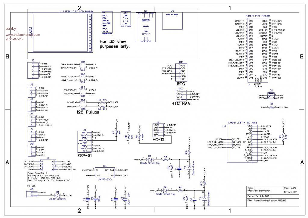 ... almost all of the Maximites, the MicromMites, the MM Extremes, the ArmMites, the PicoMite and loving it! |
||||
| Mixtel90 Guru Joined: 05/10/2019 Location: United KingdomPosts: 5720 |
I looked around for a local PCB manufacturer but no luck. For the quantities I'd be looking at its impossible to get any of them down to anything affordable. We don't really have any electronics hobbyist support in the UK now. :( If I look outside the UK then shipping costs are crippling - unless it's from China, so it would be JLC PCB for me. Hence the interest in producing designs that I can make myself in 1-off quantities. Mick Zilog Inside! nascom.info for Nascom & Gemini Preliminary MMBasic docs & my PCB designs |
||||
| panky Guru Joined: 02/10/2012 Location: AustraliaPosts: 1094 |
PCBs arrived - couple of hours and I have a fully operational Pico Backpack - very pleased to find no errors on PCB. Designed for 2.8" ILI9341 with connectors for I2C, SPI, COMs, all of which could be re-purposed in software. Also connectors for an HC12 or ESP8266. Has an RTC module but next time I might try to design for an on-board RTC chip rather than the module. The array of pads near the bottom right of the bottom picture are for analogue input and are set up as shown below. Any of the components can be changed or replaced with zero ohm resistors to allow input functions of rectify, voltage divide, integration, differentiation, clamping etc. The junction of the right hand zener and resistor goes to the analogue pin. I only use this input configuration on analogue pins 0 and 1. 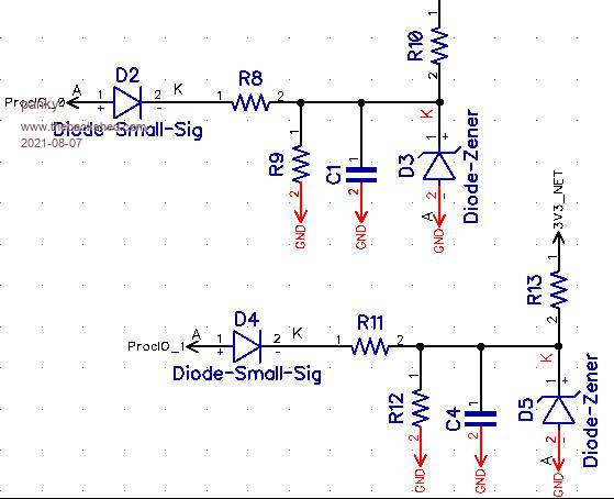 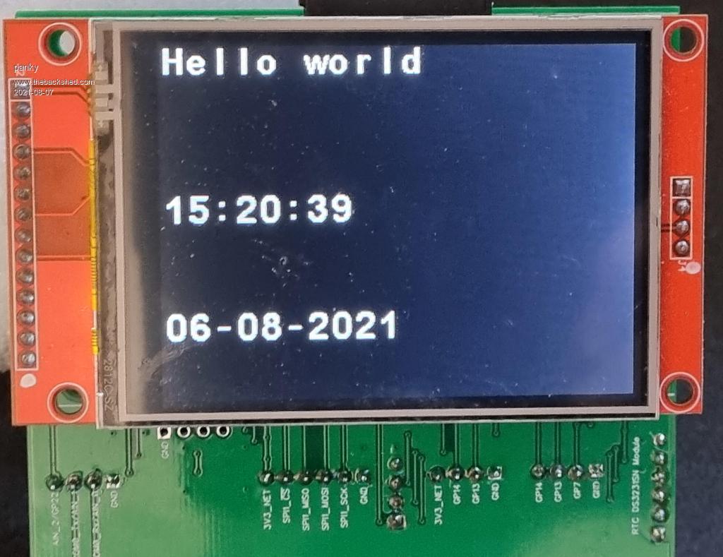 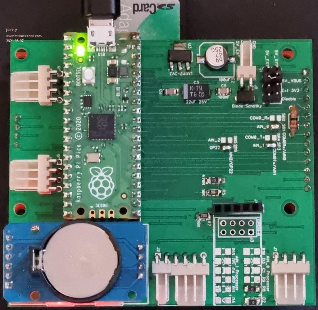 ... almost all of the Maximites, the MicromMites, the MM Extremes, the ArmMites, the PicoMite and loving it! |
||||
| Mixtel90 Guru Joined: 05/10/2019 Location: United KingdomPosts: 5720 |
Very nice, Panky. :) I like your analogue input circuit, but the series diode will make it non-linear as well as introduce volt drop. In actual fact it may not be needed for polarity protection (which I'm guessing is why you included it) as the zener will forward conduct under those circumstances, clamping the ADC input to Vss-0.6v, which you might get away with. The RP2040 spec says Vss-0.5v minimum. An even better approach, and within spec, might be to use a reverse-biased Schottky diode in parallel with R9/R12. Still waiting for my PCBs. They are completed and (slowly) on their way. I might try another version but surface-mounting the Pico. Edited 2021-08-07 18:34 by Mixtel90 Mick Zilog Inside! nascom.info for Nascom & Gemini Preliminary MMBasic docs & my PCB designs |
||||
| Solar Mike Guru Joined: 08/02/2015 Location: New ZealandPosts: 1123 |
If I can make a suggestion here: Place a reverse biased switching silicon diode across both R10 and R13 to clamp any input voltages to 3.3V + 0.6v; R8 and R11 should be large enough to limit excessive current flowing into the pin input approx 10-20k. Get rid of that zener it has too much leakage and will stuff up your ADC readings; D2 and D4 will also affect your results, if you are worried about reverse input voltages then replace the zener with a similar Si diode above eg 1N4148. Cheers Mike Edited 2021-08-07 20:36 by Solar Mike |
||||
| Mixtel90 Guru Joined: 05/10/2019 Location: United KingdomPosts: 5720 |
The ADC pins already include an internal diode to VSYS to prevent over-voltage inputs. Only a current limiting resistor is needed. Agreed, the zener would be better as a diode - but a Schottky type to keep within the Vss-0.5v limit of the RP2040. The ADC input impedance can be as low as 100k, so I don't think it would be wise to exceed 10k series resistance if you want any accuracy. Mick Zilog Inside! nascom.info for Nascom & Gemini Preliminary MMBasic docs & my PCB designs |
||||
| panky Guru Joined: 02/10/2012 Location: AustraliaPosts: 1094 |
Thanks for the thoughtful comments guys. I think you may have misunderstood how the pads might be used. The components shown are really just place holders - there isn't any case that I can think of where you would want to use all as shown. But if you had an AC signal of some sort but all you wanted to measure was the DC value, you could use the signal diode spot plus the capacitor slot and maybe the resistors as voltage dividers. If you had a DC signal in that was say 12V, you would just use two resistors as a voltage divider and either replacing other components with zero ohm resistors or leaving them out out altogether. If you had an input voltage that that had noisy spikes on it, you might want to leave the zener in as protection. Also, you could configure the pin as digital in and again use either a voltage divider configuration and/or the capacitor/zener for spike or noise suppression. All depending on what type of input signal you were trying to measure - it is intended to allow flexibility in signal processing on the board reducing the need to have some external components do the job. In my particular case, I am measuring the output from a vehicle regulator - I need a voltage divider to limit the input voltage to the Pico and also both the capacitor and the zener for noise suppression and spike protection. The input diode is replaced with a zero ohm resistor and the last pullup resistor omitted. Doug. ... almost all of the Maximites, the MicromMites, the MM Extremes, the ArmMites, the PicoMite and loving it! |
||||
| Mixtel90 Guru Joined: 05/10/2019 Location: United KingdomPosts: 5720 |
Fair enough, Doug, but the comments about the zener remain. :) If there is sufficient series resistance to protect the built-in diode to 3v3 then the input can never exceed that so the zener is superfluous. However, protection against negative excursions isn't built in, so a reverse biased Schottky diode (look for a low capacitance one, something like BAT41) instead of the zener would be a good idea. The series resistance and that diode should always be fitted really. Everything else is optional. :) I was a bit naughty and didn't include any ADC input protection at all on my backpack. That was simply because I had no space for it - it was very limiting keeping to a single-side pcb. I figured that the connector could take a sub-board with any necessary bits on so it wasn't too important really. Beware of the ADC inputs. Those on-chip diodes will let your analogue signal power the chip! Edited 2021-08-08 18:35 by Mixtel90 Mick Zilog Inside! nascom.info for Nascom & Gemini Preliminary MMBasic docs & my PCB designs |
||||
| phil99 Guru Joined: 11/02/2018 Location: AustraliaPosts: 1781 |
" Those on-chip diodes will let your analogue signal power the chip!" Have made that mistake with other MMs. If the supply to the chip at the input end is lost the protection diode tries to power everything, but not for long. :( |
||||
| Mixtel90 Guru Joined: 05/10/2019 Location: United KingdomPosts: 5720 |
Hence the current limiting resistor, Phil. :) The Pico circuit uses ADC3 to measure VSS via a potential divider but it uses a mosfet to disconnect the signal if 3v3 is switched off. That protects the input. IIRC all the PIC chip pins include those ESD protection diodes as they are formed in the substrate. They are very low current rated (it's better to put another diode in parallel with them really) and any reasonable current pushed into an input will cause trouble. The RP2040 has them deliberately formed on the ADC inputs only - they say they aren't there on any other pins, but I'm a bit doubtful. They actually return to the IOVDD pin, which is connected to VSS on the Pico although it could be to a lower voltage on some installations. Mick Zilog Inside! nascom.info for Nascom & Gemini Preliminary MMBasic docs & my PCB designs |
||||
| Volhout Guru Joined: 05/03/2018 Location: NetherlandsPosts: 3519 |
For protection a Zener has historically been used. It is a inheritance from the time we used 5V logic levels, and +/- 15V powered opamps. There is one thing you have to keep in mind though: Starting at 4.7V and upward, Zener's are silicon diodes with a controlled reverse characteristic. When a normal diode is not conduction until it's breakdown, a Zener has a controlled breakdown (at 4.7 volt for example). The "knee" (the area where isolation changes into conduction) is weak in low voltage Zener's, and sharper in higher voltages. A typical 4.7V Zener will act as a diode for negative voltages, and as a protection for 4.7V for positive voltages. There will be leakage above 4V. Zener diodes with a voltage lower than 3.9V are totally different. They are basically "stacked" diodes. They operate in forward conducting mode. These diodes (unless designed to do so) will not protect the negative going signal. And they will leak significantly when close to the Zener voltage. If you want to protect the ADC inputs, you can use Zener's, but only when the input circuit is really low impedance. (max 1k), otherwise the Zener (assume 3.3V Zener) will cause terrible a-linearity (aka "clamping") in the measurement range. If you use a 3.9V Zener this is better, but it will not protect your input in any way. Do not use Zener's to protect analog inputs. Also: do not use Schottky diodes for clamping analog inputs. If protection is need, use silicon diodes (i.e. BAV99, or even better BAV199) to 3.3V rail and GND. They come with 2 in a package, and are more or less "matched". -or- investigate the use of ESD protection diodes (such as TPD4E1U06). But again, these are typically designed for digital signals, so use the ones with low leakage, or with a Vcc connection that you connect to 3.3V. A very cheap alternative I generally use is: add series resistance. The ADC's in a pico will accept a series resistance of 100k. And if you can accept a 100pF to ground from the ADC pin (100k/100pF low pass filter), your have an inherently good protection. Make sure the 100k resistor can handle higher voltages (when it breaks down it does not protect), so use a 1206 or even MELF for SMT, or a 1/4 watt through hole or bigger. This is assuming there are weak protection diodes inside the chip. You use the 100k resistor to limit the current, so the weak internal diodes can handle the surge the energy. Edited 2021-08-09 18:18 by Volhout PicomiteVGA PETSCII ROBOTS |
||||
| Mixtel90 Guru Joined: 05/10/2019 Location: United KingdomPosts: 5720 |
I wouldn't be happy with silicon diodes to protect the ADC inputs on the RP2040. The specification is for the input to remain within -0.5v and IOVDD+0.5v absolute maximum. That more or less makes Schottky diodes the only choice in spite of their leakage, doesn't it? Vf for the BAV199 starts at 0.6v at 150C and can be over 0.8v at 25C. Input resistance of the ADC inputs can be as low as 100k, so 100k series resistor is way too high for accuracy. I would suggest 10k maximum, with schottky diodes to gnd and VSYS. I don't think there's much you can do about it other than buffer the ADC inputs. Mick Zilog Inside! nascom.info for Nascom & Gemini Preliminary MMBasic docs & my PCB designs |
||||
| Volhout Guru Joined: 05/03/2018 Location: NetherlandsPosts: 3519 |
Use silicon diodes, but add a resistor between the diodes and the ADC pin. This may still raise the voltage at the BAV199 exceeding the input pin spec, but there will be no energy in the overvoltage. Values are subject to calculation, but this is the general idea. 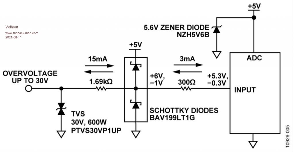 Understand that the zener at the Vcc is essential !! That is where all energy goes in the end. The BAV199 is NOT a Schottky diode. Edited 2021-08-11 00:35 by Volhout PicomiteVGA PETSCII ROBOTS |
||||
| Mixtel90 Guru Joined: 05/10/2019 Location: United KingdomPosts: 5720 |
The ADC supply on the RP2040 is IOVDD maximum (hard wired to VSYS (3.3v) on the Pico). Consequently inputs to it are -0.5v to +3.8v. The 3.3v supply is direct from the SMPS. Although the input impedance can be as low as 100k, it's almost all capacitive so you can't depend on there being any current into the ADC input. A series resistor directly on the ADC input won't work to give a voltage drop from the tap in the diodes if there's no current. :) These ADC inputs are a bit fragile really. A shunt resistor is probably a good idea. True, the BAV199 is a silicon diode, not Schottky. Consequently it's Vf is between 0.65v and 0.8v so in this case I wouldn't like to use it to protect inputs that will only stand 0.5v reverse voltage. Probably a simple circuit like a varistor followed by a simple potential divider may be all that's necessary. If the input is low impedance then it could source the reverse leakage of a schottky diode. High input impedances should be buffered anyway. Mick Zilog Inside! nascom.info for Nascom & Gemini Preliminary MMBasic docs & my PCB designs |
||||
| phil99 Guru Joined: 11/02/2018 Location: AustraliaPosts: 1781 |
It's looking like op-amp buffers may be needed to get both protection and accuracy. If sockets are used the op-amps can be unplugged to use the pins for other purposes. |
||||
| Mixtel90 Guru Joined: 05/10/2019 Location: United KingdomPosts: 5720 |
With the capacitor value bug on the RP2040 I don't think it'll be regarded as a precision ADC anyway. I'm not going to worry too much. :) Crikey, blowing up a complete Pico is way cheaper than replacing many ADC chips! Mick Zilog Inside! nascom.info for Nascom & Gemini Preliminary MMBasic docs & my PCB designs |
||||
| Volhout Guru Joined: 05/03/2018 Location: NetherlandsPosts: 3519 |
In my professional job, I just released a design using ATTINY212's as ADC's (Input voltage powered, isolated). Far cheaper than using separate ADC's. PicomiteVGA PETSCII ROBOTS |
||||
| Page 1 of 2 |
|||||
