
|
|
Forum Index : Microcontroller and PC projects : MatherpMite 1A...
| Page 1 of 2 |
|||||
| Author | Message | ||||
Grogster Admin Group Joined: 31/12/2012 Location: New ZealandPosts: 9078 |
As requested, here is a new thread on this board. Any readers NOT familiar with what this board is and how it fits in the MicroMite family, please see this thread. Current version of this board is like this: TOP COPPER: 
BOTTOM COPPER: 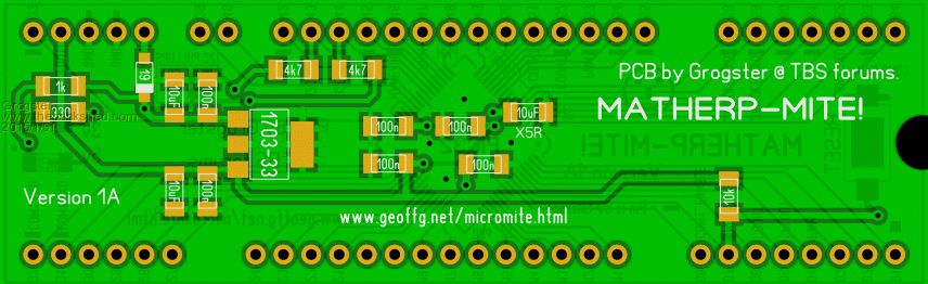
I have not yet added the header that WW wants - that's next, but this will give everyone an idea as to where we are at. @ Mick - Thank you for your suggestion on PCB size. I will take it under advisement. Smoke makes things work. When the smoke gets out, it stops! |
||||
| WhiteWizzard Guru Joined: 05/04/2013 Location: United KingdomPosts: 2794 |
G, Only observation now is to recommend two different colour LEDs! For green use GRN on silkscreen, for yellow use YEL, etc (just so it fits in the footprint as you currently have it!) If going for the SKINNY pcb option then I would recommend 2mm PCB thickness (personal experience with customers breaking 1.6mm boards even with headers along edges). Other strengthening method is to ue extra thick copper! WW For everything Micromite visit micromite.org Direct Email: whitewizzard@micromite.o |
||||
| Grogster Admin Group Joined: 31/12/2012 Location: New ZealandPosts: 9078 |
Why would you use different colour LED's? Does not bother me, but I am curious..... On the PCB thickness, I always opt for 1.6mm boards, which are USUALLY tough enough. 2mm board can be done, but it is pretty expensive to add that extra 0.4mm.... I am looking very seriously at the skinny option put forward by Mick. It will give me a chance to play again with multi-layer PCB design. If I find it too difficult, we always have the two-layer design to go back on. Smoke makes things work. When the smoke gets out, it stops! |
||||
| WhiteWizzard Guru Joined: 05/04/2013 Location: United KingdomPosts: 2794 |
So if only one is lit for whatever reason, you know which one is good/faulty! 
For everything Micromite visit micromite.org Direct Email: whitewizzard@micromite.o |
||||
| Grogster Admin Group Joined: 31/12/2012 Location: New ZealandPosts: 9078 |
Does not compute. Two red LED's, each labelled, if the one next to "5V" is out, the 5v is bad(in which case the 3v one will be off too). If the one next to "3v" is out, the 3v rail is bad. Anyhoo, here is my preliminary SKINNY footprint: 
This is also on a 2.54mm grid, but is only 12.7mm between the header pins. This PCB WILL be 4-layer at least. Smoke makes things work. When the smoke gets out, it stops! |
||||
| WhiteWizzard Guru Joined: 05/04/2013 Location: United KingdomPosts: 2794 |
It was more a thing about 'seeing' in the dark. However your answer leads to the question: why do you need two LEDs. I went through a similar 'thought process' with the led on my 44-pin module. Ended up with just one LED indicating the MPU has 3v3 power. Like you say, it will be off if there is no 5v power. No need to have 2 leds on if powering from 5v in my eyes! Hope this makes kind of sense! Like the skinny footprint 
WW For everything Micromite visit micromite.org Direct Email: whitewizzard@micromite.o |
||||
| Grogster Admin Group Joined: 31/12/2012 Location: New ZealandPosts: 9078 |
You are so right. 
One single red LED it is then. Skinny is proving a challenge, but I like "Forcing" a PCB layout to work. Smoke makes things work. When the smoke gets out, it stops! |
||||
| WhiteWizzard Guru Joined: 05/04/2013 Location: United KingdomPosts: 2794 |
Is it a 'challenge' due to available space? Or unfamiliarity of using your PCB app with a 4-layer design? You have me curious now! Please don't go smaller than 0805 SMDs!! For everything Micromite visit micromite.org Direct Email: whitewizzard@micromite.o |
||||
| Grogster Admin Group Joined: 31/12/2012 Location: New ZealandPosts: 9078 |
Available space. I've done a couple of practise 4-layer boards, but this one is a real squeeze. EDIT: - Here is the Skinny version so far. Still more work to do, but it is coming along.... 
Smoke makes things work. When the smoke gets out, it stops! |
||||
| Zonker Guru Joined: 18/08/2012 Location: United StatesPosts: 761 |
Sweet Grogs..! I am sure you can do this..! I bet you can pull the whole thing off in 2 layers... I like all "need to be close" caps on the back side of the MPU... I did the same with the LCDuMite... Lou and I want to get involved with the beta-testing on this new motor, but creating a new test fixture for the chip using other prototype break-out boards will be a kluge compared to your board... So, by the looks of it, you wont be long in finishing this up.. (sweet)... I think I will wait for your new toy to arrive... Put us on the list...! Thanks G..! |
||||
centrex Guru Joined: 13/11/2011 Location: AustraliaPosts: 320 |
Hi Grogster Looks like design by committee again some of the suggestions are ok. Going smaller than the the wide design could only mean smaller parts, someone requested nothing than the 805 smd for my tired eyes and no binocular microscope 1206 would be my smallest size. To go any smaller could end up meaning that assembly could only be done companys specializing in this sort of work. Adding to the design by committee request a gnd pin along side the the console pins would make connecting the console easy. I like the wide one if you get any made put me down for one. Regards Cliff Cliff |
||||
| Grogster Admin Group Joined: 31/12/2012 Location: New ZealandPosts: 9078 |
Hi folks. As for the DBC(design by committee) side of things, let it be known that I take all ideas on-board(no pun intended!), but it is not going to be possible to design something that will make everyone happy, so I will squeeze in what I can, and that means that some things may have to be dropped for physical restraint reasons. We'll see. The idea at this stage is that the WIDE one is the one that I will get made, as this is done and dusted, albeit wide-ish. Mick's suggestion of making it skinny made me think again, so this is why I am even attempting the skinny version. IF I can squeeze everthing into the skinny one, that will be the one that gets made. Oh, and on the SMD - nothing smaller then 1206 - that is about as small as I like to go too. 0805 is very common, but I still think that is too small!  Smoke makes things work. When the smoke gets out, it stops! |
||||
| MicroBlocks Guru Joined: 12/05/2012 Location: ThailandPosts: 2209 |
I think if you make it one unit (0.1") wider you will be able to make it a 2 layer board. I never see someone using a supervisory chip. They are great to use and take out concerns about having the right reset timings and startup delays. I find them very valuable. They are small so should not be a problem placing it. Microblocks. Build with logic. |
||||
| Grogster Admin Group Joined: 31/12/2012 Location: New ZealandPosts: 9078 |
Funny you should mention supervisory chips, TZA - the new board has one.
Here is the current version. 12.7mm row spacing, entire thing is now skinny. 4 Layer board. I will be getting some of these skinny ones made, if anyone is interested. Deliberate offset rows top and bottom on top-right of board, to prevent accidental reverse insertion in a PCB. TOP COPPER: 
INNER LAYERS: 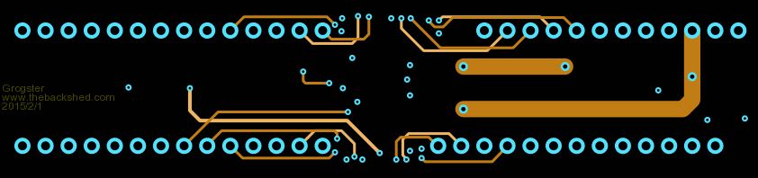
BOTTOM COPPER: 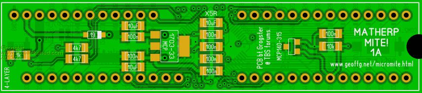
Mick was right - it could be squeezed.
No room for WW's header though, but I don't really see that as a problem - programming connections, 3v3, GND and MCLR are all easily plugged into for initial HEX programming, and then you'd use the console. Smoke makes things work. When the smoke gets out, it stops! |
||||
| matherp Guru Joined: 11/12/2012 Location: United KingdomPosts: 8601 |
Grogster Please change the name - my efforts are trivial compared to Geoff! Please put me down for a 5. Can you include the port B pinout on the silkscreen? Pins on the 64-pin chip are: 16,15,14,13,12,11,17,18,21,22,23,24,27,28,29,30 in that order (portb0..15) I really like the skinny format
Peter |
||||
| Grogster Admin Group Joined: 31/12/2012 Location: New ZealandPosts: 9078 |
It was your idea - suggest a name, and I will change it. 
I will label the port B pins, and upload another image tomorrow. Smoke makes things work. When the smoke gets out, it stops! |
||||
| MicroBlocks Guru Joined: 12/05/2012 Location: ThailandPosts: 2209 |
I would rotate the voltage regulator so that its biggest connection is not right under the PIC. Normally with 4 layers you have TOP, GND, VCC, BOTTOM. That will help a lot with crosstalk or EMC. De GND and VCC layers are often copper fills only leaving space for the signals to go from top to bottom (vias). Something to consider when signal speeds are getting higher as with this chip. 80 Mhz is very fast. Microblocks. Build with logic. |
||||
| WhiteWizzard Guru Joined: 05/04/2013 Location: United KingdomPosts: 2794 |
Hi Grogs, Even though you haven't put a USB-to-serial header on your PCB, I will still take an Airmail envelopes worth of PCBs"
How soon do you think you will send to PCB fab house? An eta to UK would be appreciated
Nice looking PCB
WW For everything Micromite visit micromite.org Direct Email: whitewizzard@micromite.o |
||||
| Grogster Admin Group Joined: 31/12/2012 Location: New ZealandPosts: 9078 |
@ TZA - I have added ground-planes to both inner layers, so that they are also copper-fill/pour where there are not tracks. All four ground-planes on all four layers, are now connected to GND. This means there is an almost full ground-plane right below the IC(inner1), and another one below that. That should suffice, yes? The only thing I see here as a possible issue, is that these ground-planes will have some capacitive effect(in that the layers themselves will form a capacitor within the PCB itself), but as all these layers are at ground potential, any capacitance should be effectively zero. Hopefully. @ WW - I will be ordering today, after I change the name(as per matherp's request) and add the legend for the 16-bit port he wanted. ETA from factory to me is about two weeks normally, then airmail to you, probably another week. Good things often take time... (and no - I have not forgotten Skype. I hope to get a phone today.)Smoke makes things work. When the smoke gets out, it stops! |
||||
| Frank N. Furter Guru Joined: 28/05/2012 Location: GermanyPosts: 815 |
@Grogster: Your design is on the right way with 4 ground planes! Spent so much vias you can place to connect these four planes together and let no unconnected isles stay around! (the best is to create fences with vias around the whole pcb to minimize EMI) Don't use thermal pads for GND-pins! - it's very bad to solder without them but it's better for a lower EMI! Frank |
||||
| Page 1 of 2 |
|||||
