
|
|
Forum Index : Microcontroller and PC projects : Sprint Layout 6.0
| Author | Message | ||||
Grogster Admin Group Joined: 31/12/2012 Location: New ZealandPosts: 9063 |
Sounds like a plan, Craig.  Yes, I always use the AutoSave feature in SL6. You should also have a UPS on your machine too if you do any kind of work on files that represent lots of hours work, but many don't. I tend to use a "Backup, backup, and then backup again" kind of triple-redundant method: 1) A copy saved to a local backup USB drive(separate from the working copy) 2) A copy saved to my NAS sitting out in the shed 3) A copy saved to the cloud. I use iDrive for my cloud storage, and it auto-syncs all the latest files and any files that have been changed every couple of days at 3AM while I am recharging myself.  Smoke makes things work. When the smoke gets out, it stops! |
||||
| Tinine Guru Joined: 30/03/2016 Location: United KingdomPosts: 1646 |
Effectively always the case; I have two Panasonic Toughbooks (internal battery) for the plant floor and for the desk, I have two Windows tablets (internal battery). Some clown here at the plant will hit the wrong breaker and kill my power but I'm never affected Craig |
||||
| pwillard Senior Member Joined: 07/06/2022 Location: United StatesPosts: 274 |
Harbor Freight Sells something similar to those for less than $50. (Though probably not as good) Habor Freight Small Saw |
||||
| pwillard Senior Member Joined: 07/06/2022 Location: United StatesPosts: 274 |
The beauty of Sprint is that if you need to do something like this... you just draw it. So 20 minutes... call it done. 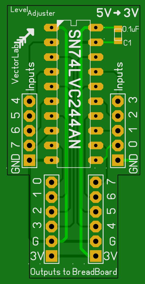 |
||||
| Tinine Guru Joined: 30/03/2016 Location: United KingdomPosts: 1646 |
Very professional  Craig |
||||
| Tinine Guru Joined: 30/03/2016 Location: United KingdomPosts: 1646 |
Meanwhile, elsewhere, "Production board just arrived": 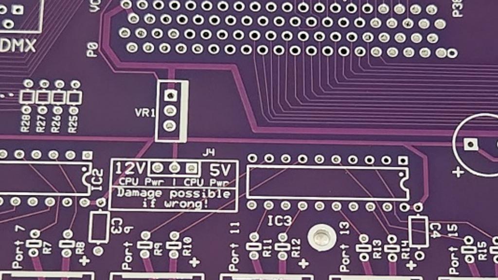 Whatever it is, I ain't buying one  @pwillard You have a white silkscreen but how'd you get the black border? Clearly there're lots of little SL6 tricks that I'm unaware of. Craig |
||||
| Mixtel90 Guru Joined: 05/10/2019 Location: United KingdomPosts: 5727 |
The "border" is a cutting line on layer O. The top silkscreen is on layer S1. I normally have layer O yellow, but you can set colours. Mick Zilog Inside! nascom.info for Nascom & Gemini Preliminary MMBasic docs & my PCB designs |
||||
| Grogster Admin Group Joined: 31/12/2012 Location: New ZealandPosts: 9063 |
Quite. I guess it will work fine electrically, but I always like to make my boards look neat and tidy. There is no electrical reason to do so, and if time is absolutely of the essence, then OK, but if you have the time, I always like to make the boards neat with equal track spacing and 45-degree track angles etc, to give the board some sense of dress. That's just me though.  Smoke makes things work. When the smoke gets out, it stops! |
||||
| Tinine Guru Joined: 30/03/2016 Location: United KingdomPosts: 1646 |
I have zero tolerance for sh*te craftsmanship. Takes the same amount of time to do a neat job. It has taken a few hours to become proficient but the grid manipulation, the Ctrl key and the Space-bar are your friends in SL-6 Craig |
||||
| Grogster Admin Group Joined: 31/12/2012 Location: New ZealandPosts: 9063 |
I find the test tool to be very useful to confirm that you have tracks connected to where they should be. I am always using that tool as I go, and it is a tool I run over every single track as a final sanity check before I order the boards. Smoke makes things work. When the smoke gets out, it stops! |
||||
| Tinine Guru Joined: 30/03/2016 Location: United KingdomPosts: 1646 |
LOVE the test tool Meant to ask....what approach do you take with 4-layer boards? Craig |
||||
| Mixtel90 Guru Joined: 05/10/2019 Location: United KingdomPosts: 5727 |
I'll third the test tool. :) Also, click the Solder mask button before you run a CRC check for Silkscreen on pad. You can instantly see if you've got it on a pad (where it matters) or a via (where it may not matter). Mick Zilog Inside! nascom.info for Nascom & Gemini Preliminary MMBasic docs & my PCB designs |
||||
| pwillard Senior Member Joined: 07/06/2022 Location: United StatesPosts: 274 |
Right, I use alternate colors. |
||||
| Grogster Admin Group Joined: 31/12/2012 Location: New ZealandPosts: 9063 |
It depends on what I am doing. Generally, if I need a lot of tracks in a small space, then four-layer is the way to go. The default industry standard, is to use the inner layers as ground and power planes, but I tend to use the inner layers for signal tracks, and keep the top and bottom copper layers with a ground-plane. I find that works superbly well for shielding, but this is not set in stone - it all depends on what I am doing. I don't think there is any law to four-layer boards, just whatever works best for you at the time. As mentioned, it is pretty much a default design standard with four-layer, to use the inner layers as ground and supply, but you don't HAVE to do that. Not sure if that answers your question - "What approach do you take" could be interpreted in different ways. Smoke makes things work. When the smoke gets out, it stops! |
||||
| Mixtel90 Guru Joined: 05/10/2019 Location: United KingdomPosts: 5727 |
I've not tried 4-layer yet, but I think I would probably go for: C1: short traces and links between pins I1: ground plane I2: power plane C2: remainder of traces This gets the little connections that get in the way clear of the longer runs. It also puts the ground plane as close as reasonably possible to the active devices. Having the ground plane and power plane adjacent gives distributed capacitance, which usually helps a bit with supply decoupling. Obviously any layout is going to be a balance between these, but I think it might be a good starting point. Always a good idea to bring anything important on the inner layers out to test points. :) Remember, JLCPCB can't do blind vias - they always go right through the board no matter which layers they are joining. Mick Zilog Inside! nascom.info for Nascom & Gemini Preliminary MMBasic docs & my PCB designs |
||||
| Grogster Admin Group Joined: 31/12/2012 Location: New ZealandPosts: 9063 |
Good point.  I knew there must have been a good reason for the "Default" of ground and supply on the inner layers, but I could not think why that was, so there you go. Smoke makes things work. When the smoke gets out, it stops! |
||||
Quazee137 Guru Joined: 07/08/2016 Location: United StatesPosts: 522 |
pwillard hope you haven't got the Harbor Freight one yet. � I got it and it ruff on PCB's. � This cost more but I love it. � �PCB Saw � I got it when cutting 200 panelized boards 3 to a board to fit DIN rail boxes. � The 3rd blade in from the left works GREAT. �Quazee137 Edited 2022-10-03 17:19 by Quazee137 |
||||
| Tinine Guru Joined: 30/03/2016 Location: United KingdomPosts: 1646 |
This is what interests me the most because I work with a lot of high-power PWM (servo amplifiers). Craig |
||||
| Solar Mike Guru Joined: 08/02/2015 Location: New ZealandPosts: 1123 |
Careful with high power on 4 layer pcb's, the inner layers are generally 0.5oz copper so very thin (unless you pay a lot extra); thus don't handle large currents very well. For high current pcb's the outer layers are better for large current handling and better cooled. For cutting PCB's a 30 cm long handle metal shears (big tin-snips) cut it like a hot knife through butter. Cheers Mike Edited 2022-10-03 17:49 by Solar Mike |
||||
| Mixtel90 Guru Joined: 05/10/2019 Location: United KingdomPosts: 5727 |
@Craig A few thoughts on noise... Most noise is transferred over power rails. If you absolutely have to take control power from the load power rail (because it's from a charger/battery setup for example) then filter it, fit a transzorb (or preferably several in parallel) to kill the biggest spikes then follow by a linear regulator. It doesn't need to drop a lot of voltage, but they usually have very good noise rejection characteristics. After that keep your load and "clean" supply wiring several inches apart (or screen the wiring from your clean supply). Keep low and high current grounds completely separate, as far back to the source of supply as possible. If the drive circuit itself requires any appreciable current (e.g. a MOSFET driver) then try to route the supply to the drivers back as far as possible to your PCB supply and don't forget the power rail decoupling. Where the power device is off your PCB get it's drive signal connection as close as possible to it's driver as you can - keep lead lengths short as fast edges over lengths of wire will transmit unpredictably at RF frequencies. Data lines are better using something like CAT5 than ribbon cable or loose wiring. The return path, twisted with the signal path, helps reduce common mode noise. Opto-isolation is nice but isn't usually necessary unless your supplies have to be isolated - and if you have to have a common ground for protection purposes, for example, it's only marginally effective anyway. Some spikes will cross the capacitive gap in an opto coupler if it can respond fast enough. Mick Zilog Inside! nascom.info for Nascom & Gemini Preliminary MMBasic docs & my PCB designs |
||||
