
|
|
Forum Index : Electronics : a new way to balance lithium ion battery
| Author | Message | ||||
| wiseguy Guru Joined: 21/06/2018 Location: AustraliaPosts: 995 |
Yahoo - I obviously did a crappy job of reading - last night I re-read what you wrote and realised I had misinterpreted your post and what you were saying - I should have posted that then. My background is calibration, a single end point calibration is usually a nono,a mid point calibration is usually better if you cant do a 2 point calibration - with that crap floating in my head I lost the plot & read what I expected.... Thanks to Warp too, I had no idea of the speed that the potential of a cell can suddenly rise, at the end of charge - forewarned is forearmed - I have no intentions of "helping" anyone at this early stage of learning to adjust their system. There are many pitfalls & lots to learn. My experience with batteries (to date) is that they resemble the "rock of Gibraltar" and have huge inertias with regard to attempts to change potential. The balancing system I was suggesting/proposing would have the ability to transfer imbalance charge many times better than A "flying capacitor" system - I was addressing that point, but it seems there are a lot of other factors beside balancing that need to be monitored & taken into account. Thanks again for valuable feedback. If at first you dont succeed, I suggest you avoid sky diving.... Cheers Mike |
||||
Madness Guru Joined: 08/10/2011 Location: AustraliaPosts: 2498 |
Best and only way to treat an EGS002 nicely is to leave it in its antistatic bag if it came in one. At least they are cheap. There are only 10 types of people in the world: those who understand binary, and those who don't. |
||||
| Warpspeed Guru Joined: 09/08/2007 Location: AustraliaPosts: 4406 |
I am just starting out too. I have a battery bank, and have built a BMS and a charger but its not yet hooked up and doing any work. The reason for that is my current solar system is positive ground, running at around -220 volts dc. My battery and new inverter will be around +110v negative ground, so nothing is compatible. There will be a grand changeover day in the near future, with a quick solar panel rewiring job. I have so far carried out a few battery charge and discharge tests just to get the feel of things, and the way the cell voltages behave is a lot more dramatic than I was expecting. As the cells are expensive, and I am told can be permanently damaged by a one time mishap, a great deal of caution is required with multiple layers of quite independent protection. Cheers, �Tony. |
||||
| Solar Mike Guru Joined: 08/02/2015 Location: New ZealandPosts: 1123 |
This balancing method as suggested by wiseguy is really interesting, and with an immediate requirement for a solution, had a quick think and come up with a circuit that might work. Requirements: 1: Each battery cell to have a small push pull inverter, synchronised to all other cells in the bank, thus when the outputs are coupled in a common AC buss will push power back into lower capacity cells by synchronous rectification. 2: With only 3 - 3.6 volts per cell, a suitable drive mechanism has to be used that works at this low voltage. 3: Pulses driving each mosfet have to be identical width and with sufficient dead time to ensure transformer volt seconds are not exceeded, otherwise flux walking leading to transformer saturation will occur. 4: If sync pulse widths are variable, then effectively this will determind current transfer rate between cells. A TL494 can be used as a suitable pulse generator when used in manual mode, here a pwm frequency can be easily set with an RC period and the dead time varied by manually setting the voltage on the DTC pin, voltages between 0.5 to 3.5 volts set the pulse width 97% to 0, there will be no overlap between pulses and they are identical widths. Whatever battery cell management system is used, when it detects a cell >= set balance voltage then it can set a suitable voltage on the DTC pin to start charge transference across the bank. With 12 volt supply 4 led drivers could be placed in series, so a 16 cell bank = 4 x 4. Higher voltages would allow more boards placed in series for each pulse train. 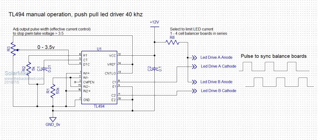 On each cell balancer board a 1 watt 12 to 12 volt isolation converter can be used to power the gate driver, the FOD3180 has a fast opto interface and sufficient drive current for the mosfets. Using separate pulse drives common to all boards will keep everything synchronized. Warp mentioned transformer drive and this would simplify things somewhat; but maybe harder to implement in getting identical suitable pulse transformers for DIY use. 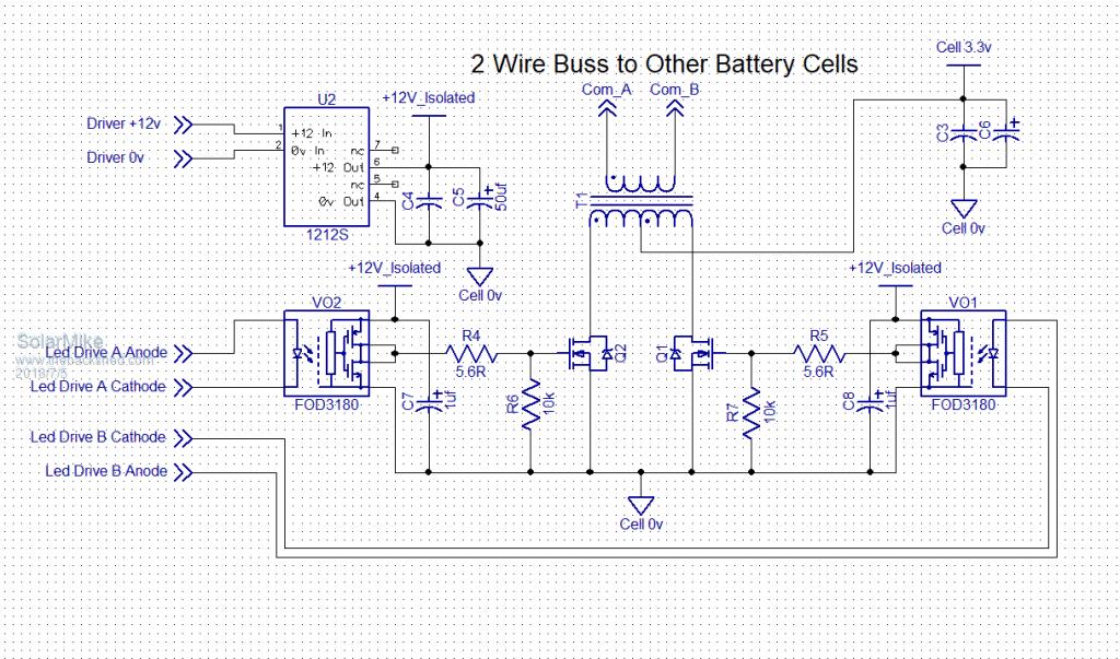 Cheers Mike |
||||
| Warpspeed Guru Joined: 09/08/2007 Location: AustraliaPosts: 4406 |
I really like the idea of variable duty cycle, that is something I had never considered. Opto isolator drive as you are suggesting will have fewer problems and be much easier to get going than pulse transformers. For the gate drive dc supply, how about a Maxim MAX630 running off the cell voltage? https://pdf1.alldatasheet.com/datasheet-pdf/view/73626/MAXIM/MAX630.html That would reduce the required external wiring slightly. The whole idea Wiseguy has proposed is a very intriguing idea, which has opened up a great many possibilities. Cheers, �Tony. |
||||
| Solar Mike Guru Joined: 08/02/2015 Location: New ZealandPosts: 1123 |
The Max630 would work as a power supply chip, similarly you can purchase 2-6v input to 12v fingernail sized up converters all ready to go on ebay etc for a couple of dollars. However I dont like powering items directly off each cell in the bank as the power drawn by each device may differ and so unbalance the system over time. If they are all powered by a power rail derived from the whole battery, then this cannot happen, an extra pair of wires daisy chained between each balancer pcb hopefully wont be an issue. I have some very old 40AH cells here that are on their last legs, they vary between 50% and 80% capacity and would be ideal for testing, so might make something up and give it a go, see what ideas wiseguy or anyone else comes up with first... Cheers Mike |
||||
| Warpspeed Guru Joined: 09/08/2007 Location: AustraliaPosts: 4406 |
If you are only going to test with just a pair of cells initially, the very first prototype need not be galvanically isolated. The negative sides of the two cells could be commoned, and then the gate drive need not be isolated. Just needs a pair of push pull transformers to couple the power across, or even just one transformer to start off with. Trifilar windings on a small pot core perhaps ? Cheers, �Tony. |
||||
| wiseguy Guru Joined: 21/06/2018 Location: AustraliaPosts: 995 |
HaHa very witty Mad - your humour is similar to mine. My intention is to build an inverter 250W @ 12V in, with a Toroid (~9V - 230V) and suitable choke and give it a hard time & do a lot of CRO investigation to see what makes the thing tick (not just the 3 musketeers ticks - they will get investigated too). To start with I will only use 4 FETs - 1 for each leg of the "H" with attention paid to short runs for Gates & corresponding Sources etc. I have (at last count) 11,500 200V 33A mosfets so I shouldnt run out of FETs anytime soon. I know this is not duplicating in any fashion the high power inverters and the grief they are giving to some in these forums (I do agree BTW its undoubtedly the poor gate drives & long wires that has plagued most constructors) but it will allow me to characterise all the waveforms and how the EG8010 really works with little risk - and as a grey nomad caravanner I want a small sine inverter for little tasks whilst travelling so the effort wont be wasted. I may start a thread on it if I (or anyone requests) as I think it might be interesting for others. I want to use a bipolar drive system but in a slightly different way - if it is possible with the EGS IC. Once I am happy with that then the fun will really begin...... If at first you dont succeed, I suggest you avoid sky diving.... Cheers Mike |
||||
| Madness Guru Joined: 08/10/2011 Location: AustraliaPosts: 2498 |
With a conservative main breaker and totem pole or similar driver chips the EG002 should be immune from blowups as Warp mentioned. Since I have used Totem pole drivers I have not had one IR2110 driver chip fail, neither have the TIP41c and 42C transistors in the drive circuit. But you do need to do the mods to the EG002 to prevent it blowing your MOSFETs to pieces. There are only 10 types of people in the world: those who understand binary, and those who don't. |
||||
| wiseguy Guru Joined: 21/06/2018 Location: AustraliaPosts: 995 |
Solar Mike, FYI I am posting a few parts of schematics I have used for similar applications. The first is for transformer gate drive - if you use 50/50 drive a single transformer can do both push and pull. This would not be my preferred choice. The PN2907 works adequately when used with IRF3205/3206 Fets. Some dont appreciate the value of this simple circuit. When the Drain is switched high at first power application (on/off switch turn on), any gate charge (from drain/gate coupling capacitance) attempting to lift the gate V(+) & turn on the Fet, biases the 2907 into conduction clamping the gate very solidly at 0.6V. As the emitter (tied to the gate) attempts to rise, the gate series diode (between B&E of 2907) is reverse biased and the base 2k2 is held to source potential (-) turns on the base of the 2907 solidly. When a genuine (+) signal from the drive transformer arrives at the base of the 2907 it is turned off (reverse biased) and the gate diode turns on the Fet as usual. 10K gate resistors to ground (source) will stop a gate from turning on from slow charge build up but do almost nothing to quench fast (+going) drain transients which can- apart from turning on a Fet unintentionally - also cause the 20V gate barrier to get punched through killing or crippling a FET unless a zener or this type of circuit is used. It also allows a very fast gate turn off when the drive signal turns off. Before anyone points out that the zener is on the wrong side of the gate diode to clamp a gate transient, its purpose is to clamp any switching spikes coming from the drive transformer that could exceed the gate max voltage. For a 3V application this is probably overkill & not really needed, I just use it as standard in a lot of my gate drive apps. I always use 50/50 (ok 49.9/49.9) duty cycle for power switching when I can, it avoids walking fluxes saturating etc. I use turns ratios for changing DC levels & I supply the bridge/push pull circuit with a current controlled PWM drive. I am not saying PWM wont work here but my experience & intuition tells me to avoid PWM in this type of application. I do encourage experimentation and building on this idea and making it better, however if PWM becomes the choice I dont want to be associated with any negative issues or downfalls that may flow from that choice. If it works, that's great someone else deserves and has earned the kudos - I just do what I can do and make work - I know my limitations and what I believe I can achieve. A simple series R, 0R1 to 0R01 should limit circulating currents to reasonable values. For a cell mismatch of 0.2V the 0R1 allows ~ 1A to flow, if you use 0R01 ~ 10 amps would flow. 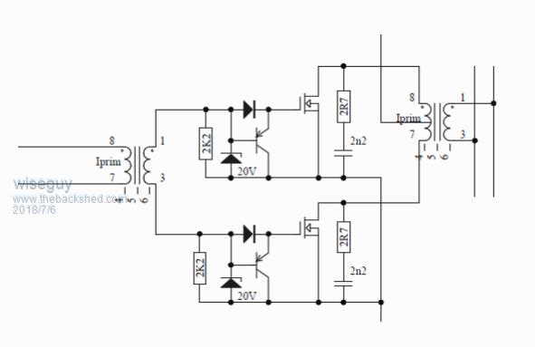 I think that using the cells to power each converter would work ok - I was researching a suitable logic gate Fet, some give quite good performance at 3V gate drive. I was investigating/planning to use the H11 fast optos which work at 3V and a gate driver IC that works at 3V - I have been researching stuff as time presents - which is not often enough lately. I prefer the active gate drivers and optos to transformers - this is a personal choice & also for safety isolation with those big nasty cells. For push pull I was thinking the UCC2808 for its complimentary drive, all optos could be driven in parallel from the one master. Its only issue is it needs ~ 4.5V to start operating. I have used plenty of NME12/12 for gate isolated drives over the years they work a treat. Warps boost type converter could power the master or maybe a simple plug pack at 6+ volts could also act as a suitable on off switch (from a management system?) and avoid boost converters etc I have run out of time tonight for other circuit bits - later .... stay tuned. If at first you dont succeed, I suggest you avoid sky diving.... Cheers Mike |
||||
| Warpspeed Guru Joined: 09/08/2007 Location: AustraliaPosts: 4406 |
Thanks Mike, some rather original thinking there. That gate clamp is a particularly interesting circuit, especially for higher voltage applications. It certainly beats the ubiquitous 10K or 4K7 gate to source resistor that most people seem to use for that purpose. Never really thought much about it before, but super low logic level mosfets are going to be a lot more vulnerable to the evil turn on spike. I came up with an idea recently how to provide very simple opto isolated gate drive, incorporating pretty foolproof cross conduction protection, particularly high noise immunity, and adjustable dead time in a very simple way that may be of interest. The main purpose of this (at the time) was to give highest noise immunity for some rather remote gate drive for multiple mosfets in a high power environment, and protection during initial power up and power down from spurious turn on caused by unpredictable logic events. 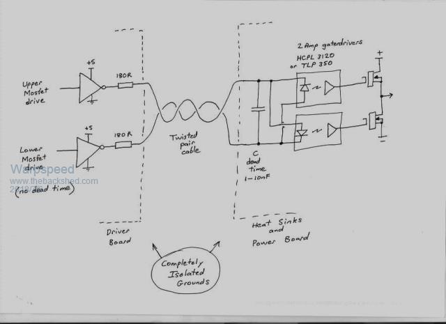 Something similar may have application here, as we will be dealing with some very low impedance sources and loads, rather long wiring, and any brief noise event on the common gate driver bus could be catastrophic. A very simple bipolar drive straight from a flip flop without any dead time could drive a large bus with many opto isolators. Cheers, �Tony. |
||||
| wiseguy Guru Joined: 21/06/2018 Location: AustraliaPosts: 995 |
Warp, That looks like an interesting LED drive proposal - I will have a play with it sometime - I did not use it as I cant vouch for its performance & it appears it would need a pair of totem drivers to drive properly and the TL494 is just O/C. I have created an untested schematic that I am confident will work perfectly in the balancer. As drawn it could take a complementary drive signal from Solar Mikes TL494 proposed schematic. Suggested Frequency of operation from 25kHz to 100 KHz - I tend to keep my circuits in the 25 - 50kHz for lower switching losses. The deadtime should be set to near minimum for the best performance/efficiency. I forgot to mention that the drive circuit arrangement that protects the FET from fast Drain positive transients that could try to turn on the gate has another function. When the drive signal - in this case from the OPTO - is removed a very fast turn off occurs as the gate charge is dumped via Q3/4. 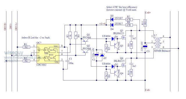 The circuit draws ~ 1.5mA from the cell when there is no drive signals - this is from the Optocoupler idling current @ 3V. When the circuit starts diodes D3/D4 scavenge Vcell x 2 from the opposite Fet drain that turned on to enhance the drive circuit to ~ 6V for best gate drive & FET performance. As drawn there would need to be 1 circuit including the 1 x transformer per cell. If an AC bus is to be used the secondary does not need a centre tap. If DC is to be used on the common current share bus (RHS) a duplicate circuit would need to be connected to the other side of the transformer and driven from the same opto drive signals and the Cell+ and Cell- on the RHS circuit would be the + & - DC share. If 1 transformer was required for say 4 cells, the transformer could use 4 identical windings and 4 of the cell circuits as above for isolated 4 cell balance. A 5th winding would share the balance current to another 4 cell boards 5th winding Phase matching is critical so note starts & finishes and direction of winding and polarity of drive signals. The 5th winding if centre tapped could also have the above circuit for a common DC Bus. I estimate the parts to be ~ $6per cell circuit (without transformer cost). An ETD34 or ETD39 should easily handle shunt balance currents of up to 10 - 20A Note no gap in the transformer - it is not storing energy but transferring it. Although I specified surface mount FETs there are plenty of through hole (TO220)types that perform well with gate voltages of ~5V that will switch up to 100A for just a dollar or so, but be aware some have high gate capacitance and perform better ~ 25 - 40 kHz. If at first you dont succeed, I suggest you avoid sky diving.... Cheers Mike |
||||
| Tinker Guru Joined: 07/11/2007 Location: AustraliaPosts: 1904 |
Possibly a nice way of balancing for 4 cells but for my 16 cells it has way too many parts for a one off construction. Now, if you get one going and then get it mass produced so it can be bought for a price similar to those little DC/DC converters on a PCB..... Meanwhile I'll stick to my working constant voltage current injecting system to keep the cells balanced. Its only a smallish current but running it 24/7 does the trick. Klaus |
||||
| Solar Mike Guru Joined: 08/02/2015 Location: New ZealandPosts: 1123 |
I have amended my original circuit for generating suitable drive pulses, the TL494 really requires a low impedance totem pole buffer to drive many parallel leds correctly. It is not good practice in this situation to switch leds off by leaving the circuit open, as this allows long floating connecting wires that can easily be affected by localized interference. The low impedance buffer output shorts the input to 0 volts when its turned off. I have only suggested a TC4427 here as it contains dual buffers and I happen to have some to use up. The whole circuit could be simplified if variable pulse width isn't required, by using a flip flop driving a buffer, providing Warps dead time circuit is used. 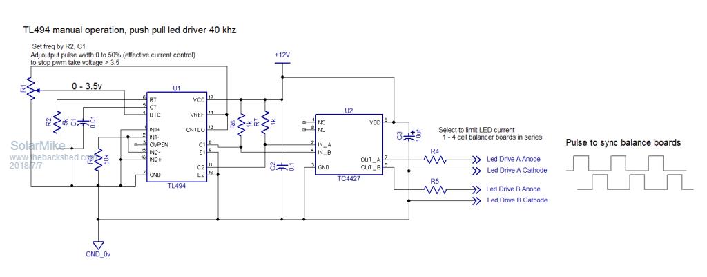 Wiseguy your circuit is intriguing and I happen to have a few of those ETD39 cores here. For another suggestion, for the low powers we have here 30-40 watts couldn't we just use a self driven ringing choke inverter and isolated output winding + diode to feed current into the whole bank; with start control via a cheap opto-coupler, no driver required; would simplify everything. [Edit] oops, the TC4427 should be an inverting type TC4426. or swap its input resistors to emitter follower to use the one in the circuit. Cheers Mike |
||||
| wiseguy Guru Joined: 21/06/2018 Location: AustraliaPosts: 995 |
Klaus I am sorry if the circuit intimidates you - for me its easy....... & I hate mechanical clicky things. I think I will create a PCB for an application that could also suit you that will look after 8 cells per PCB as I am sure I will be needing & using some myself. I Would be happy to give you a couple of boards for evaluation when finished & tested - if you are interested/game. SolarMike, Please note my previous post & intention to use a totem pole output single chip solution. I ran out of time earlier today to create & present my solution for the master driver. In retrospect it was probably a mistake to even mention your TL494 circuit. 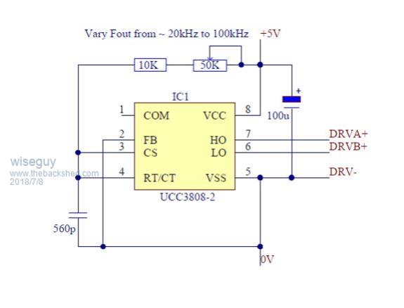 The 3808 has 500mA source and 1A sink. Each Opto can work happily from 1.5mA source current. We could drive a couple of hundred if we had to from the one master. I do not advocate driving any optos in series, I would stick to only parallel for this application. I am not certain whether Pin3 (CS) works best at GND or tied to the clock pin, I seem to remember an issue in the past - will tell you after I lash one up again. Would be happy & interested to see your suggested circuit to "use a self driven ringing choke inverter and isolated output winding + diode to feed current into the whole bank; with start control via a cheap opto-coupler, no driver required; would simplify everything". I'm not even sure I actually understand/follow the topology of what you are proposing & how the individual cells would track evenly. If at first you dont succeed, I suggest you avoid sky diving.... Cheers Mike |
||||
| Warpspeed Guru Joined: 09/08/2007 Location: AustraliaPosts: 4406 |
Agree that mosfet gate driver chips make very good opto isolator drivers. And that the opto islolators need to be positively turned off. As already mentioned, we need to drive multiple opto isolators, possibly sixteen or more in parallel, so the individual LED current limiting resistors need to be located with each opto isolator, and the common gate drive bus needs to be a low impedance voltage source derived from a flip flop to assure exactly equal duty cycles. My previously suggested opto driver scheme offers the slight advantage of requiring only two wires. And it does in fact work as advertised, requiring zero dead time from the driving source. About 2.2nF directly across each LED pair will provide a few hundred nonoseconds of dead time to start off with. It also offers a further advantage that if either of the two wires come adrift somewhere, the whole thing stops. With three drive wires, if one side of the push pull fails to switch, the transformers will saturate and *bang*. Its a possible failure mode worth thinking about. I like the scheme of using the output transformer as a cell voltage doubler, very clever. As long as the circuit can start up with only 3v, which it easily should, then it gets to run at +6v or more, for better gate drive turn on. An excellent idea. As Klaus points out, building a full initial working prototype is going to be a lot of work and use up a lot of parts. It does not look like much, but as I discovered building multiple iterations of my 30 cell balancer boards, its probably not the best way to initially start off with a project like this. We only really need to test and measure charge transfer between a pair of real cells to get an idea of what may be required, and to test some magnetics, and decide on a suitable operating frequency and impedances. To do all that we do not need to have fully isolated cells. Everything could be ground referenced for the very first attempt at this. My gut feeling is that the impedances are all going to have to be extra low to get enough useful energy flow where the voltage difference between cells might be only a few tens of millivolts. Massive fault currents are possible, some suitable fusing may be worth a thought. Anyhow with just two cells (ground referenced) we can charge one, or discharge the other and see how well they follow each other over time, and get a much better feeling for the whole concept before going to the circuit board stage. 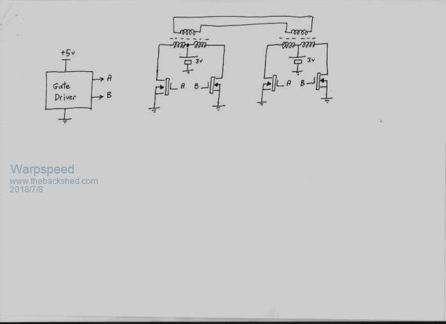 Cheers, �Tony. |
||||
| wiseguy Guru Joined: 21/06/2018 Location: AustraliaPosts: 995 |
If at first you dont succeed, I suggest you avoid sky diving.... Cheers Mike |
||||
