I'm currently building\installing a pumping control system using 2 x 12v series lead acid batteries that power a 300W 24v DC water pump. The setup has 3 x 180W PV panels paralleled, have had these panels for many years unused sitting under the house, was going to use a simple PWM controller, however the panel spec's have a high mppt voltage of 36V @5 amps, so a lot of power will be wasted, a fully synchronous controller will be more efficient.
Have made a few of these in the past, but its always nice to improve upon a previous design, so this is V1 of the idea. The design automatically senses the charge current and when it gets very low, it changes mode to asynchronous operation, turning off the synchronous mosfet and using its body diode as the buck rectifier. This prevents any possibility of the active rectifier mosfet acting as a boost converter at lower duty cycles and blowing up the buck components. This is transparent to the CPU, so I can use slower CPU software - Picaxe Basic- 20X2 running at 64 Mhz; PWM is 10bit 64Khz. Have most of the software written and it seems to be working pretty well.
Am using 2 mosfets for the PV-Battery isolation switch, Buck stage and active rectifier, so 6 in all; the mosfet specs - bulk electro's determine the max input voltage and current etc. As it stands 40 amps charge current would be the limit using 1oz pcb. The PV setup for the pumps could generate 20 odd amps, have being doing testing with 30 or more amps for 1/2 an hour and the small heatsink gets mildly warm, haven't measured the actual efficiency yet.
Have gone away from building very high current controllers, its makes more sense to split the PV up into smaller arrays each with their own controller.
I want to use this board for some other projects using 200V PV and 100V Lifepo4 batteries, so track spacing 1.6mm would handle the higher voltages.
The mosfet driver circuitry has been placed on a small sub pcb that connects using a 10pin IDC ribbon connector, the pcb sits atop the mosfet leg pins, soldered to the legs protruding through the main board. This arrangement allows the high mosfet currents be isolated away from drive signals that now go direct to the mosfet pins, seems to work very well.
Here are some photo's, will add more as testing progresses.
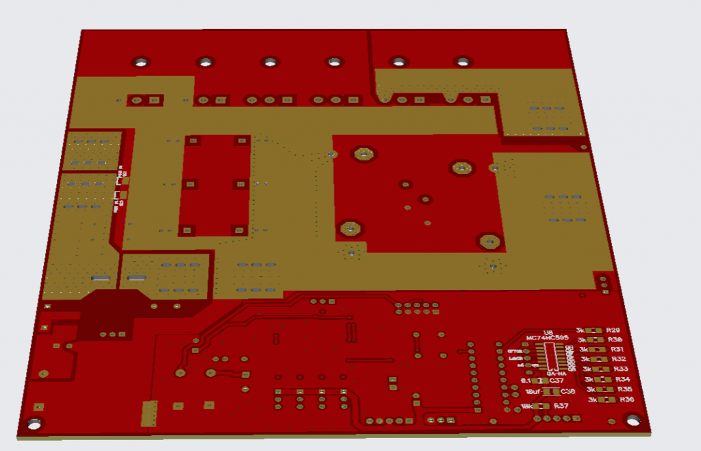
Main PCB 162 x 173mm:

Driver:


Assembled:


Cheers
Mike


