Quite a bit of inverter building has been posted about here lately so I'll add my 2 cents worth

.
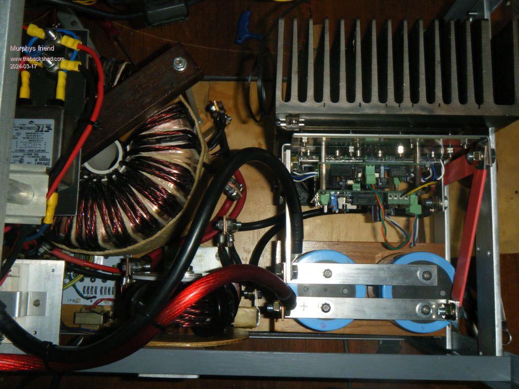
I was facing a stack of parts removed from my jinxed warpinverter and thought I could build an inverter or two from these.
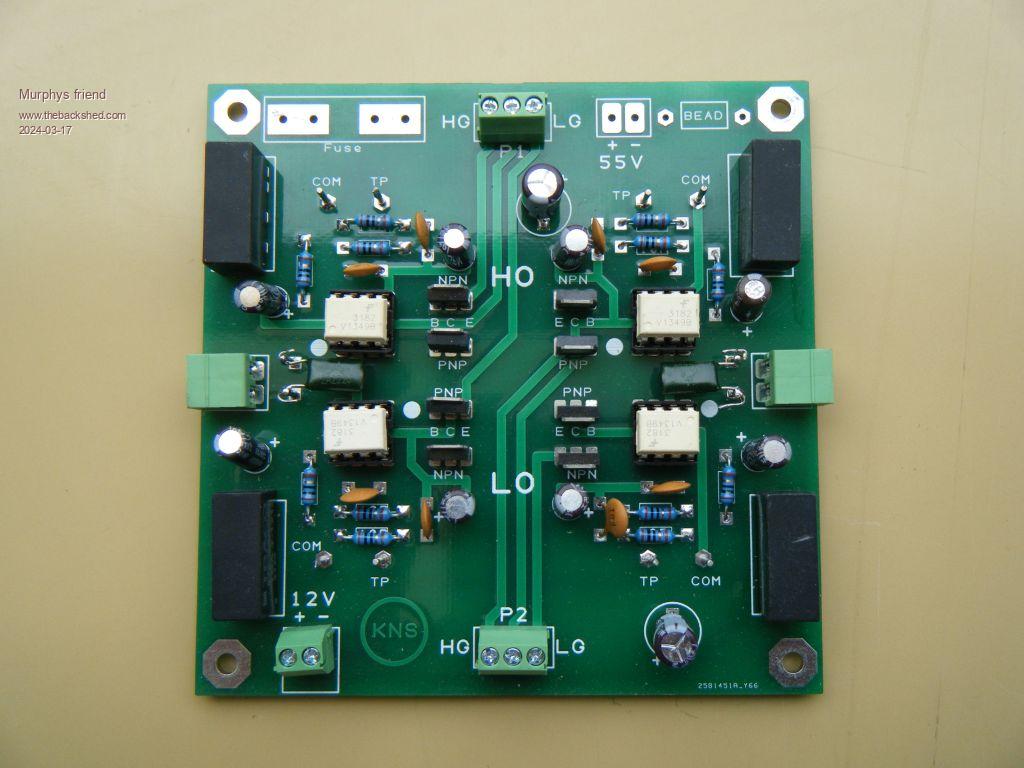
It is a very basic (no bells & whistles) EG 8010 based design, since I still have a few of those chips from my early inverter building days.
I do like the power PCB on heatsink approach Mike posted about but add my own bag of tricks.
A big expense of a decent size inverter is that large 2oz copper PCB for the mosfets & capacitors.
So, if I told you that I just built a 6KW inverter using 1oz PCB board for the mosfets you possibly won't believe that.
But, with the right track layout, making the top & bottom power tracks identical, one creates 2oz copper tracks by paralleling those tracks. This has the added advantage of these tracks having now twice the surface area for even higher current capacity.
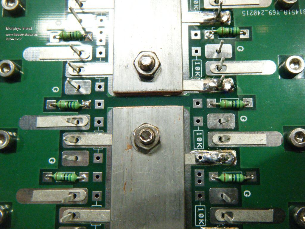
So, here is what this power PCB looks like for 12 HY5608 mosfets:

The top and bottom side are shown next to each other.
Ther is still the track bottle neck where it narrows to connect the mosfet pins to take care of.
For this I use warpspeeds trick of cutting the tail off long tail solder lugs. The next picture shows that arrangement.
Anybody considering this, make sure they are tin plated *copper* lugs (dull silvery finish) and not nickel plated brass (shiny finish) which is useless for this application.
A tip about soldering these lug tails: I have 2 sets of 60 W temperature controlled soldering irons and neither of them was up to the job with the biggest tip available. There is simply not enough heat storing capacity in those thin walled 6mm tips those irons usually come with.
I use an old fashioned non temp controlled 80W iron with a decent 10mm copper rod wedge tip. So, if it takes you longer than 2 seconds to fully flow the solder around the mosfet pins & solder lug, a more suitable soldering iron is recommended.
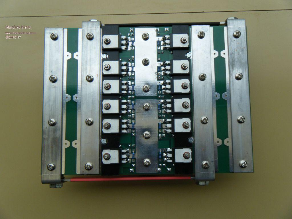
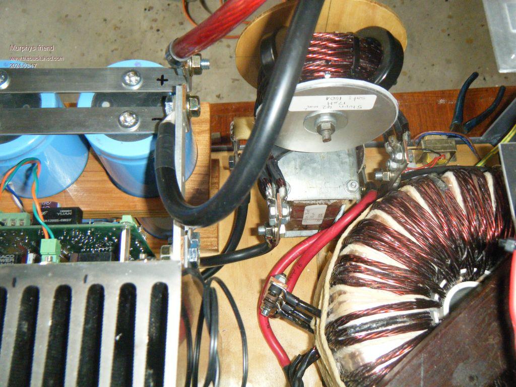
The next picture shows my power connections to the PCB tracks. I am not a fan of those dainty 6 legged, solder on PCB, screw connectors. They make it too difficult to route 32mm sq power cable & lugs to, this is much easier off the board where I can use 8mm bolts to make that connection.

Another thing you'll notice is the complete absence of the driver components, I find they clutter up space there and make the board bigger than it needs to be. It's, IMO, much easier to use a piggy back PCB for that which can have equally short gate tracks.
The only small parts on that power PCB are the gate & source/gate resistors.
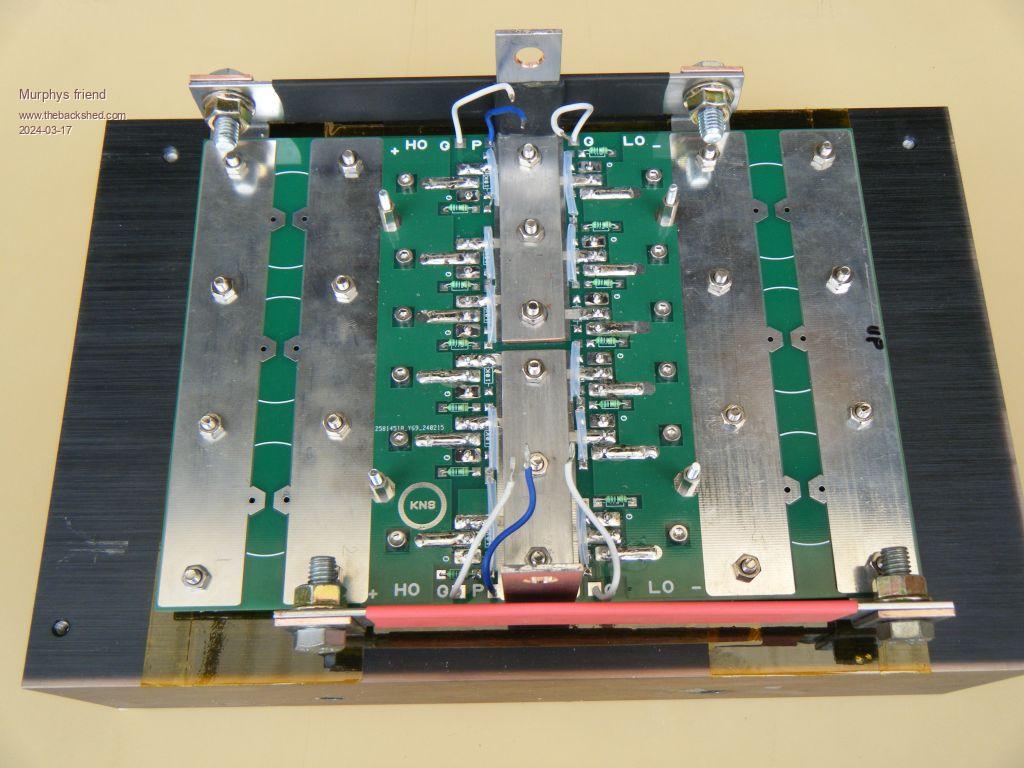
The following is a picture of the bottom side of the assembled power board. Note, there are no fancy mosfet leg gymnastics required to accommodate the ferrite beads. Just bend the legs at a right angle where their size reduces.
You may not see it clearly (its black) but I placed the mosfets on a 3mm thick fibreglass board spacer strip, between the mosfet top and PCB, to increase the gap between the heatsink & board to 6 mm. This also gives me clearance for the copper busbars (20x2mm) plus better air circulation under that board.
I designed that board for an Aerosharp heat sink but then realised I had an equally suitable heatsink from an old GTI which had a thick side fin, making it very easy to mount it with 2 x 8mm bolts in my inverter case.
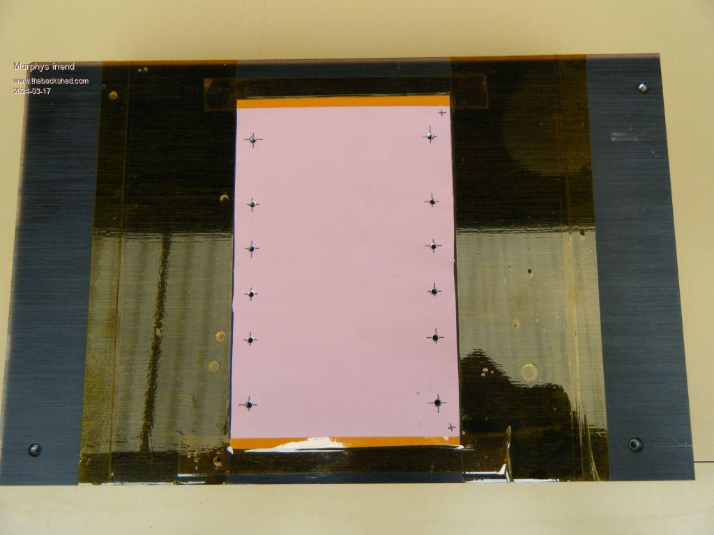
The heat sink uses a silicone sheet to isolate the mosfet drains, this is taped in place with Klapton tape.
This is much easier than using individual mosfet insulators which would be difficult to keep aligned when the board is mounted onto the heat sink.
To be continued


 .
.


 . Got to keep busy doing something I enjoy doing in my retirement years.