Guru
Joined: 12/08/2011
Location: AustraliaPosts: 332
| Posted: 03:30am 24 Dec 2023 |
Hi All
Many thanks for your detailed reply.
With the lack of interest in this thread, I HAD to spend weeks learning what you have detailed.
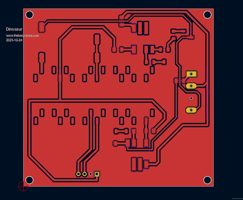
For the single layer board I changed nearly all my components to SMD.
As a result of that I used the F_Cu top layer as my routing "image"
Days of googling found what I thought was great program "Line Grinder"
https://www.ofitselfso.com/LineGrinder.php/
But it created a large circle of very dense routes in the middle of the gcode.
No matter what I tried , couldn't get rid of it.
Tried emailing, but after a day or two came back undeliverable.
So, settled on KiCad --> .gbr plot --> gbr2ngc , then to view on an online simulation https://ncviewer.com/
Yesterday tried routing it onto a piece of laminated chip board, and it was so painfully slow.
With gbr2ngc you can add g0 and g1 speed settings, so will try again after Christmas.
With the sharp 30 degree routing bit, I was impressed with the accuracy and definition.
The other item of interest was that Kicad draws a rather complex pad if that pad is in the middle
of the gnd fill. These take a long time to route.
So by editing the pcb footprint (not the library one) I could simply delete these pads as the legs
of the components (or resistors) will solder directly onto the Gnd fill area.
Even though I did not include the Edge Cuts layer in the plot, gbr2ngc will draw the outline of the board
and the circles for hand drilling.
The Rpi Pico headers were a bit more challenging, but by bending every pin left or right, I can
surface mount the header and it will be quite stable. You can see the header footprint on the pic below,
but minus the deleted pads.
Anyway a long rant in reply, but I am ready to put this to copper.
PS: Hope you are safe from the fires.