Guru
Joined: 11/02/2018
Location: AustraliaPosts: 2610
| Posted: 03:27am 09 Mar 2024 |
Less tidy but easier leg bending?

Guru
Joined: 13/10/2014
Location: AustraliaPosts: 1872
| Posted: 04:32am 09 Mar 2024 |
Thanks Phil, you saved me the trouble, a slight adjustment to that could work for the flat heatsink mounting when not using heat bars, as in this compact build.
The PCB drain hole is just past the end of the wide part of the drain lead. I just bent an old FET and it's a tight fit when sandwiched between the heatsink and PCB as the bead has to remain horizontal and the drain lead has to bend back a little more under the bead.
I may try to fit them just to see if it makes a difference when I get a chance.

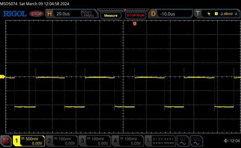
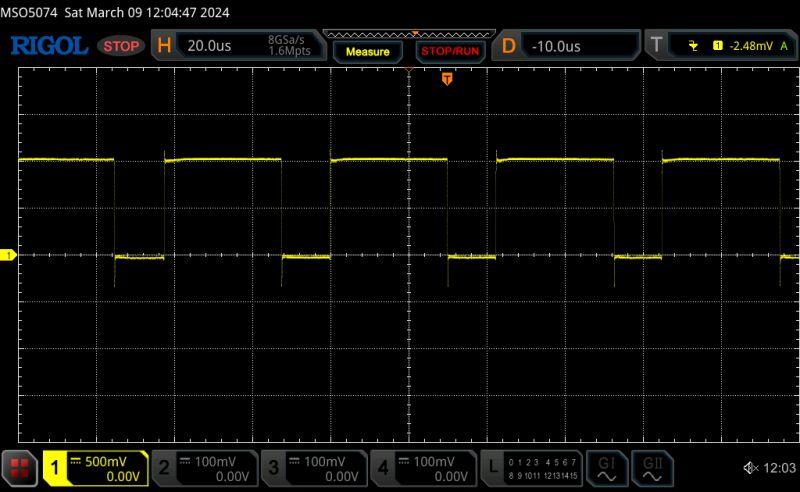
Running 250w load, same result unloaded, with incorrect chokes and standard ground clip on the CRO lead, so induced spikes and noise. Not sure they will make any difference.
Measured across the terminals T3 - T4.
Edited 2024-03-09 14:33 by KeepIS
Guru
Joined: 13/10/2014
Location: AustraliaPosts: 1872
| Posted: 02:12am 10 Mar 2024 |
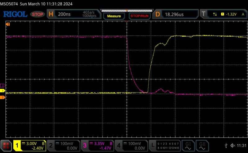
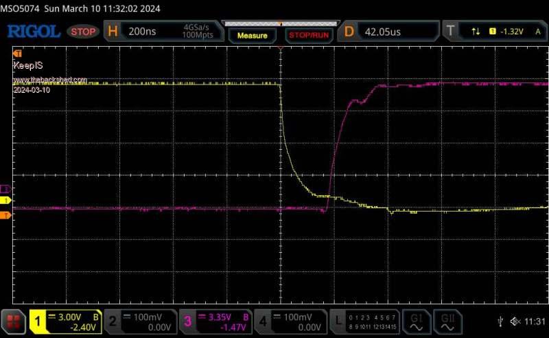
A DSO capture of the dead time, I calculated 123nS and it's pretty close.
Inverter Power board into a 100w load, a standard CRO probe on one side (yellow) and a differential probe on the other (pink).
there is some common mode interference on the CRO probe, a few clip on toriods reduced it a bit, still not ideal but I was mainly interested in the looking at the dead time for any glitches etc.
Measured between the Gate and Source at R26 -T4 and R28 - T2 (-48V) I did not have a probe setup to measure across the resistors, very tight space there when the Cap boards are on and the inverter is running into a load.
Guru
Joined: 21/06/2018
Location: AustraliaPosts: 1206
| Posted: 02:30am 10 Mar 2024 |
Mike is that measured at the gates or the actual rise and fall of the FETs ?
I am assuming gates ? Perhaps adding another 50nS would not hurt anything and give a little more breathing space, that looks a bit tighter than expected ?
To clarify for others my definition of dead time is roughly the time taken between say the gates of the upper FET turn off and the Lower Fet turn on, and vice versa. But the FETs have a delay and fall and rise time - it is possible for the gate waveforms to look about right but the actual Drains on or off from the conducting state may be quite different causing the "dead time" to actually be reduced.
I used 1n5 caps in mine and with the 240R total in series it calculates to ~ 300nSecs.
I dont have any screen shots to refer to though and dont remember what it was, I will look again in due course. Having too much fun with the paperwork

Guru
Joined: 13/10/2014
Location: AustraliaPosts: 1872
| Posted: 02:43am 10 Mar 2024 |
The original circuit has 100R series, the latest one from you has 120R and with a 1nf
cap and 5V is around 123nS,
4KW Nucleo PWR R2 Circuit.pdf from early 2003.
BTW That also shows the upper ferrite beads removed.
This was basically measured across the resistors (R26, R28) gate drive IE:
Before the 2R2 - that's means the thin PCB gate drive track. Not directly across the FET D and S.
Edited 2024-03-10 12:44 by KeepIS
Guru
Joined: 21/06/2018
Location: AustraliaPosts: 1206
| Posted: 03:10am 10 Mar 2024 |
There are (or should be 2 x 100/120R resistors in series so the calculated time I think should be roughly double ?
As time and experimentation has evolved a little since the early posting of circuits it is timely that in this current topic, hopefully I will better standardise on the values of the parts used.
The HY5608 gates in my current build uses 1R2 - their input capacitance is ~ 15nF compared to the original HY4008 ~7.4nF and now I routinely use beads on all SPWM FETs.
Edited 2024-03-10 13:24 by wiseguy
Guru
Joined: 13/10/2014
Location: AustraliaPosts: 1872
| Posted: 04:02am 10 Mar 2024 |
If you have a revised circuit I will use that as a basis, otherwise I will change the 2R2 values to 1R2 and add the upper beads to the circuit.
I understand the propagation delay in FET On/Off time. The delay shown in the capture is around 180nS, that's between the Upper and Lower FETs driven by OC1 and OC2, 1LO and 1HO, measured after the associated buffer / totem pole.
Should I open that out to 230nSec ? I can do that when I swap the 2R2 resistors out.
I can easily calculate the R value and measure the result. I should be able to quickly check the FET Gate / Source point directly with no load and no heatsink after the mod.
Guru
Joined: 11/02/2018
Location: AustraliaPosts: 2610
| Posted: 04:25am 10 Mar 2024 |
A possible way to measure the deadtime at the actual Source / Drain output may be to disconnect the transformer and connect a pair of resistors to one output. One to B+ the other to B- (a series string of automotive globes may work, or if more current is needed a pair of heater elements. Many fan heaters have 2 1kW elements. = 57.6Ω each).
During the deadtime the output voltage should be steady at Vbat / 2.
Guru
Joined: 13/10/2014
Location: AustraliaPosts: 1872
| Posted: 04:56am 10 Mar 2024 |
Thinking the same thing, I was just calculating a value and I should have a suitable power R for that. I just finished swapping in the 1R2's. Will get back to it tomorrow, and that will basically be the fine tuning done.
Guru
Joined: 13/10/2014
Location: AustraliaPosts: 1872
| Posted: 10:49pm 10 Mar 2024 |
Surprisingly there was little benefit to waveform noise when not running with the Toriod.
A bleeding obvious tip to make it easier to Probe the Inverter for various measurements when experimenting or repairing is to relocate the Cap boards.
Simply move the Capacitor boards to the left and right one mounting hole so they hang over the edge.
I have test Cap boards with small value caps to reduce the available explosive charge when testing or modifying. Still enormous energy though, even in smaller value caps.
As always, remove the cap boards and run from a current limited supply for the initial per-launch power up and final tests.
Guru
Joined: 13/10/2014
Location: AustraliaPosts: 1872
| Posted: 02:28am 11 Mar 2024 |
Wiseguy (Mike) 120R changed to 190R.
Same Probe positions as before, inverter and toriod - Idle @ 17 watt
120R
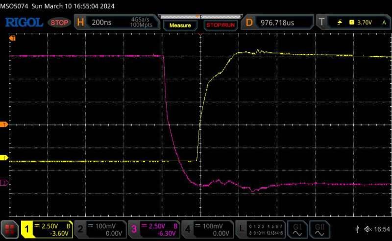
190R
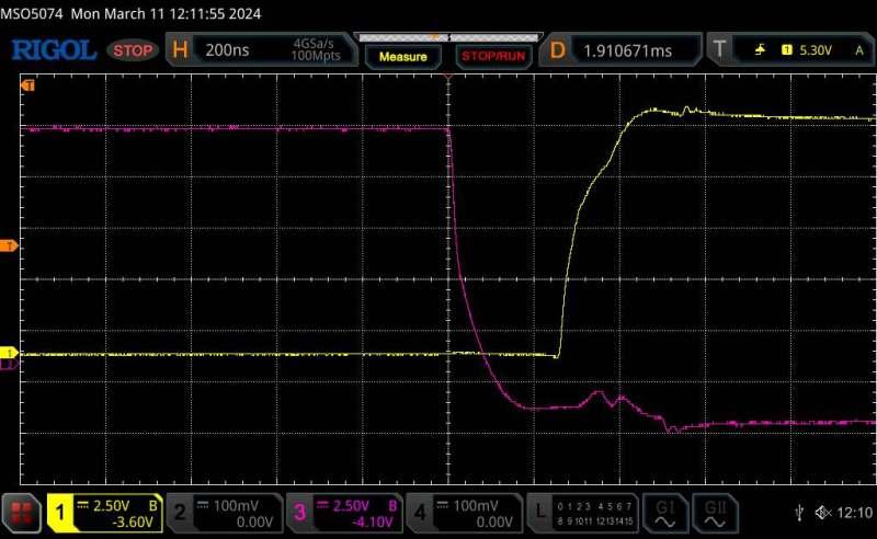
120R
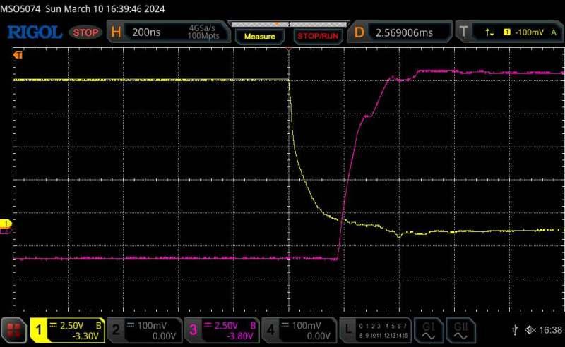
190R
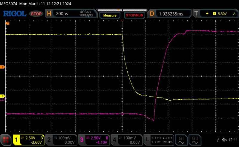
.
Edited 2024-03-11 12:36 by KeepIS
Guru
Joined: 21/06/2018
Location: AustraliaPosts: 1206
| Posted: 03:18am 11 Mar 2024 |
Mike, the 120R resistors should stay at that value and the cap gets changed for timing, that way we stay closer to being well within the max & min safe LED operating current range.
But good shots - I didn't notice the neg offset in the previous pics ?
Guru
Joined: 13/10/2014
Location: AustraliaPosts: 1872
| Posted: 04:01am 11 Mar 2024 |
OK, the first discussion hinted at increasing this slightly, so no problems, I'm glad I tried a slightly increased value as it helps to see the effect of the change for people new to this.
The negative offset - yes Dumbo here is so used to not having negative offset that I just adjusted the input looking at the waveform

A few years ago when I built the first Power board and inverter, I could not get anything above 12v in isolated supplies, so no neg offset used. I now have quite a few of the different supply types including 15v after my last order.
BTW I love the stability of this DSO, those waveforms are just captures of real time display, not zoomed out of a large buffer capture, it just locks solid. It's a shame they loose contrast when captured. One button push on the DSO to capture to a USB drive plugged into the DSO, or the DSOs internal drive. I guess most are like that anyway.
BTW the DSO is not an MSO5074 - it's fully optioned out to 380Mhz with every option.
.
Edited 2024-03-11 14:06 by KeepIS
Senior Member
Joined: 11/01/2024
Location: PolandPosts: 101
| Posted: 08:57am 11 Mar 2024 |
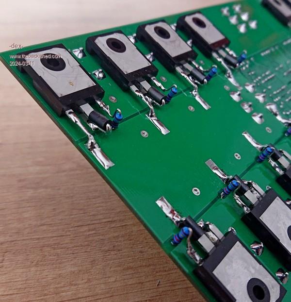
I did that. But I like the wiseguy idea better
Guru
Joined: 13/10/2014
Location: AustraliaPosts: 1872
| Posted: 11:04am 11 Mar 2024 |
The problem, as I said previously, is when you try and mount that onto a big flat heatsink, the resistors and the beads must be below the top surface of the FET.
IE It must be below the thickness then the FET body.
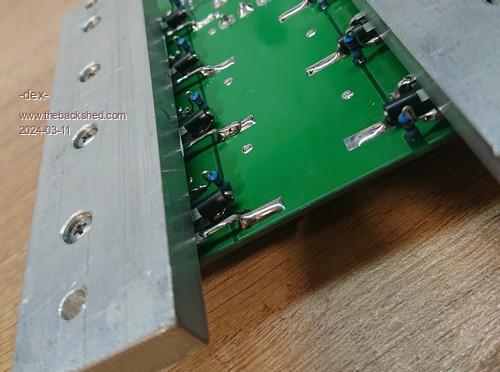
Wiseguy and I mounted the FETs on thick intermediate narrow heat bars in the first builds.
Not everyone may want to do that, this build is mounted straight onto a big heatsink.
Those resistors would also bend and short out.
.
Edited 2024-03-11 21:06 by KeepIS
Senior Member
Joined: 11/01/2024
Location: PolandPosts: 101
| Posted: 12:22pm 11 Mar 2024 |
Exactly as you're saying. I also use an aluminum bar, and in fact, if we want to install fets without it, putting the ferrite beads in this place is impossible.
Senior Member
Joined: 11/11/2021
Location: United StatesPosts: 148
| Posted: 08:49pm 11 Mar 2024 |
Great to see another build. What's reason for not having the gate resistors on the PCB?
Guru
Joined: 13/10/2014
Location: AustraliaPosts: 1872
| Posted: 10:47pm 11 Mar 2024 |
The track for the gate drive is narrow (on purpose). The layout and narrow Gate tracks maximizes the high current Drain and Source areas of the board. The resistor is right at the shoulder of each FET Gate pin.
IMHO it makes removing a FET, if ever needed, even easier, and the Gate pin is not soldered through the board, so the narrow gate track is not compromised when removing a FET.
.
Edited 2024-03-12 08:49 by KeepIS
Guru
Joined: 13/10/2014
Location: AustraliaPosts: 1872
| Posted: 10:55pm 11 Mar 2024 |
Yes that is true for the Upper FETS, the lower FETS can easily have the ferrite beads fitted, as I posted earlier, that removes over 90% of the ringing from the waveform.
FYI My main inverter, running continuously for a long long time, and absolutely abused as a test build of wiseguys design, does NOT have any ferrite beads.
BTW That looks like a nice build of the Board

.
Edited 2024-03-12 08:59 by KeepIS
Guru
Joined: 13/10/2014
Location: AustraliaPosts: 1872
| Posted: 04:36am 12 Mar 2024 |
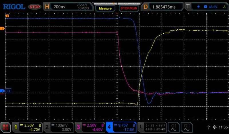
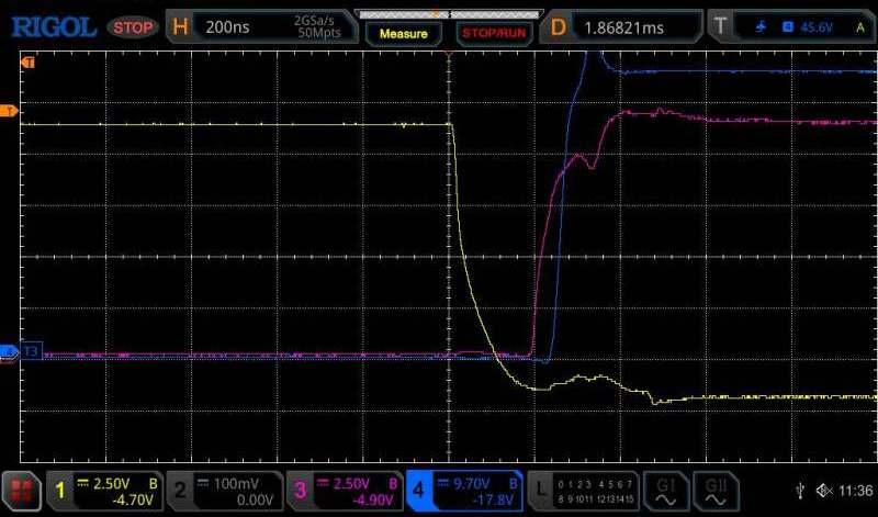
Mike (Wiseguy) While waiting for the Nano boards to arrive, I reverted to the standard chosen dead time TC and grabbed a few captures of HI and LO G-S along with the half bridge output voltage.
Poida posted something similar when he was investigating Dead time and switching waveforms around 4 years ago, in "Various aspects of home brew inverter", dam time fly's.
Inverter and toriod but only 2000uF DC filtering, No Load. 50V Rail. Incorrect Chokes (rough test setup) waiting for two cores.
DSO Traces, apology for dim colours.
Blue: Bridge out to Toriod.
PINK: HI side Gate and source.
Yell: LO side Gate and source.
2X Standard CRO Probe connections (Not ideal or even good but, whatever)
Pink is 100mHz differential probe. Other channels bandwidth limited to match.
.