Guru
Joined: 21/06/2018
Location: AustraliaPosts: 1206
| Posted: 12:44am 09 Mar 2024 |
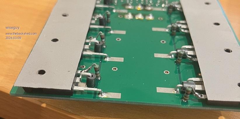
When I made my FET boards I ground a pair of pliers to create the bend of the wide shoulder of the drain leg about half way down its length - very close to the FET. the other Bends are less critical but must be close enough for ~ 4-5mm of the Drain leg to pass through the circuit board. In doing so we ensure the high current is not relegated to flowing through the plating of the inner holes from the top side to solder side.
I also made a Jig to bend the Low side FETs D & S legs, note the Drains are short and Sources are long on the Topside and reversed for the low side (Drains long Sources short). This method also will only work when the aluminium interface bar lengths are fitted, as direct fitting to a flat surface will undoubtedly interfere with the bend of the Drain Legs that protrude past the Fets heatsinking face.
Also note the gate resistors standing on the edge which is fine with clearance of the bar mounts. If mounting to a heatsink direct they need t lay flat as in one of Mikes earlier pictures.
Ok more clearly seen in this picture
Edited 2024-03-09 10:47 by wiseguy