Guru
Joined: 21/06/2018
Location: AustraliaPosts: 1210
| Posted: 03:35am 22 Apr 2024 |
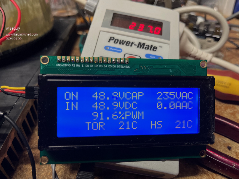
Here are some pictures, first is the inverter operating display. Note the % of PWM on the 3d line is overwritten by fault/error messages if they occur. It is informative to note, if you multiply the Vin by the % ie 48.9 x 0.916 the answer is 44.79, that is the actual DC input voltage where my inverter drops out of AC regulation with no load. If you put 44.8V in it will be at 99%
Then some pictures of the small Nano interface PCB I made cause I like neat tidy stuff. The LCD board will be in its 3d revision when it is next ordered.
I will be supplying them for 50c ea with orders. Bad news is you need to run a jumper wire from +5 to pin 15 and join pin16 to ground if you want the backlight to work, this is for the first 20 odd display boards shipped out, after that it will be the new Rev.
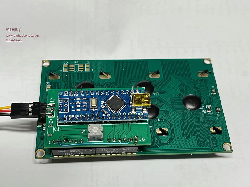
The astute readers will notice that the black wire is shown deftly plugged into the +5
pin, I just plugged it in for the picture, it wont work very well if you actually do this.....
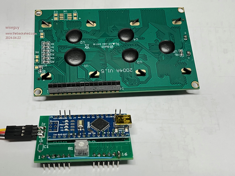
The third revision (I start at Rev0 so board shows Rev2) is as pictured below, you will see there are two pads that can be solder bridged to enable the backlight. In a typical room the black on green displays are quite readable with no backlight, but the blue displays really need one. Some LCD modules do not use a current limiting resistor, and their LEDs are directly on pins 15 & 16. So if you have one of those LCDs a suitable value SMD part (or through hole part - a bit fiddly!) can be soldered to the pads. Suggest starting with 470R and adjusting up or down as required. Both the recent ones (Blue and Green) I bought from different Ali suppliers had the current limit resistors fitted as standard.
Although I show a plug in connector fitted to the display module it makes the interface board feel a little "wobbly" when plugged in, I think the interface PCB should be soldered direct to the display but spaced from the back of the LCD by at least 5 or 6mm. The 3 pins for J1 can be soldered vertically - or as I have done, horizontally.
The board can be constructed using just the 2 x 15 rows of pins the Nano PCB's are supplied with and the little dual row header is not required to be soldered to the Nano if you buy them unassembled. Not all pins of the Nano or LCD are required to be connected so by cutting 3 lots of 6 pins 2 of 3 pins and 1 each of 4 & 2 pins. Some of the Nano pins are not required but the spare connectors were used for good stable anchoring.
Edited 2024-04-22 13:58 by wiseguy