Guru
Joined: 02/02/2017
Location: AustraliaPosts: 1432
| Posted: 11:32am 13 Mar 2019 |
Part 28: Gate drive on Madness's power board. This uses on board transistor totem pole drive
After building one of Madness's boards, I wanted to see the high and low side gate drive, focusing in particular on any signs of shoot through.
Here are the results.
Oscilloscope probe technique is important and I examine this later in the post.
I look at gate drive voltages at 2 portions of the AC output sinewave just as I did
in post #26
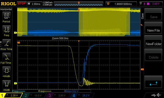
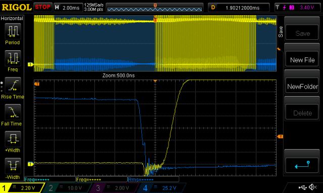
Looking at some location quite early in the 1/2 sine wave, we see
high side switch ON and high side switch OFF.
There seems to be a small degree of shoot through, the HY4008 specs say
Vgs(th) can be as low as 2V and up to 4V. We see peaks well past 2V, into maybe 2.4V.
I call this as getting to conduction on the low side MOSFETs during a high side switch ON event.
This is far less severe than what I show in post #26.
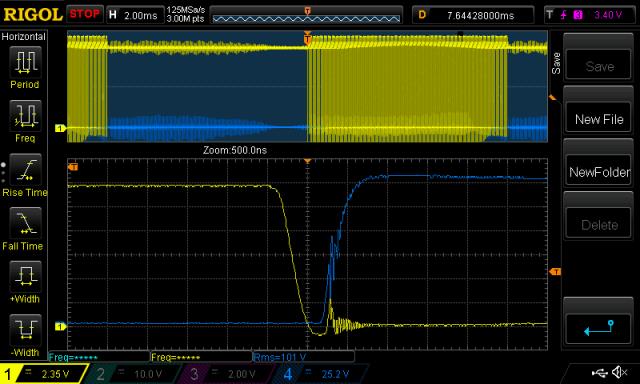
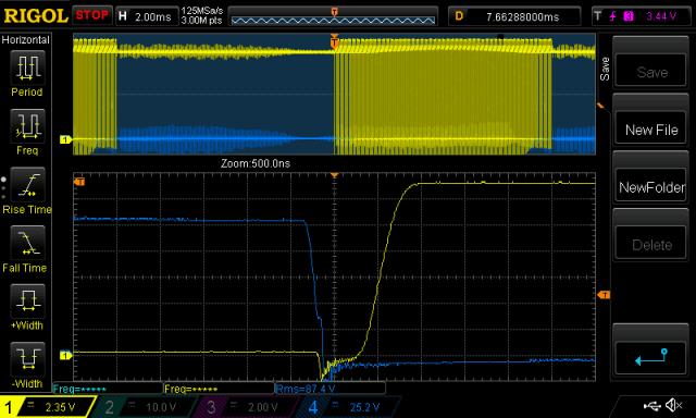
Yellow is LOW side gate drive
Blue is HIGH side gate drive.
I forgot to reset the probe gain in some of these. It is either 20x or 200x.
and
These following 2 are late in the same 1/2 sine wave of the AC output.
Less issues to my eyes and again we can see a clear effect of dv/dt on the low side gate. It can be drive negative just as easily as it can be driven positive.
and
Some of the high frequency oscillations we can see everywhere are real.
And some are due to the probe technique I used.
I use the short 5 inch long alligator clip earth leads nearly every time.
I used them in the above DSO traces.
These short earth leads are an inductor and they create high frequency oscillation
due to the approx 15-20pF capacitance of the probe and other parasitics combining
to make an LC tank.
Better probe tech. is to not use the earth lead.
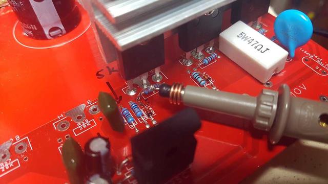
See how I do it. (only good for LOW side gate probing)
I solder two small wires on both ends of the 20K gate to Source pull down resistor.
I then poke the probe in these two springs.
This is a very good way to minimise to a large degree the effect of the 5" earth leads.
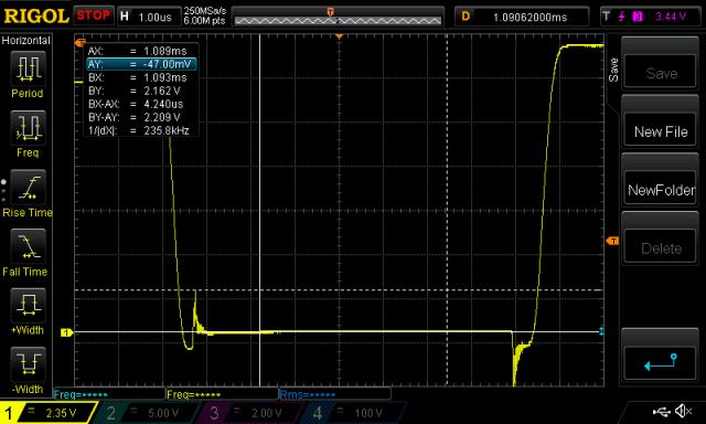
Let's look at a LOW side switch off and on event with this probe tech.
First that near the start of the 1/2 sine wave
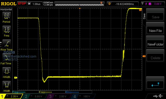
and that near the end of the 1/2 sine wave
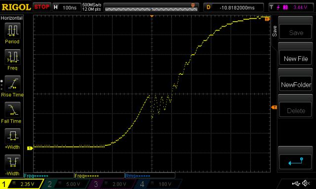
Zooming in to the right hand side rise event we see some oscillation, at about 6MHz

I feel this could be improved, no idea how.
The value in reducing this is the MOSFET's could spend less time in the switching stage and more time either fully on or fully off. This will reduce heat, stress, increase inverter life and improve overall efficiency
In case you think this is some poor DSO interpolation artifact, here are the data points at each sample time. 500MHz sample rate.
Yeah, yeah, probe compensation. I could/should do that and calibrate things and
rent special test gear and, and...
I need to show you other comparisons of with and without the little earth lead. Most striking is to do this on a digital output pin on an Arduino or Raspberry Pi or STM32 or something. It's night and day.
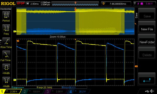
Finally, a capture showing the gate voltage behaviour during a few PWM cycles.
We can see the peak gate voltage sag a little but this can't be any problem.
It is hardly surprising Madness's power boards work so well. They reduce, by quite a lot, the shoot through I see in power boards using IR2110 gate drive ICs directly to power MOSFET gates (e.g. Alliexpress inverter boards, Ozinverter designs, etc.)
Wiseguy has some alternate power board designs in progress and I look forward to seeing how his go. They use closely located drive ICs and opto couplers. Maybe these will reduce even more the dv/dt effects?
I may be repeating myself here but I must say:
This is fun.
wronger than a phone book full of wrong phone numbers