Notice. New forum software under development. It's going to miss a few functions and look a bit ugly for a while, but I'm working on it full time now as the old forum was too unstable. Couple days, all good. If you notice any issues, please contact me.
Solar Mike Guru Joined: 08/02/2015 Location: New ZealandPosts: 1162
Posted: 04:28am 09 Jan 2021
Copy link to clipboard
Print this post
Started a new topic for this build to separate from the 08M2 version.
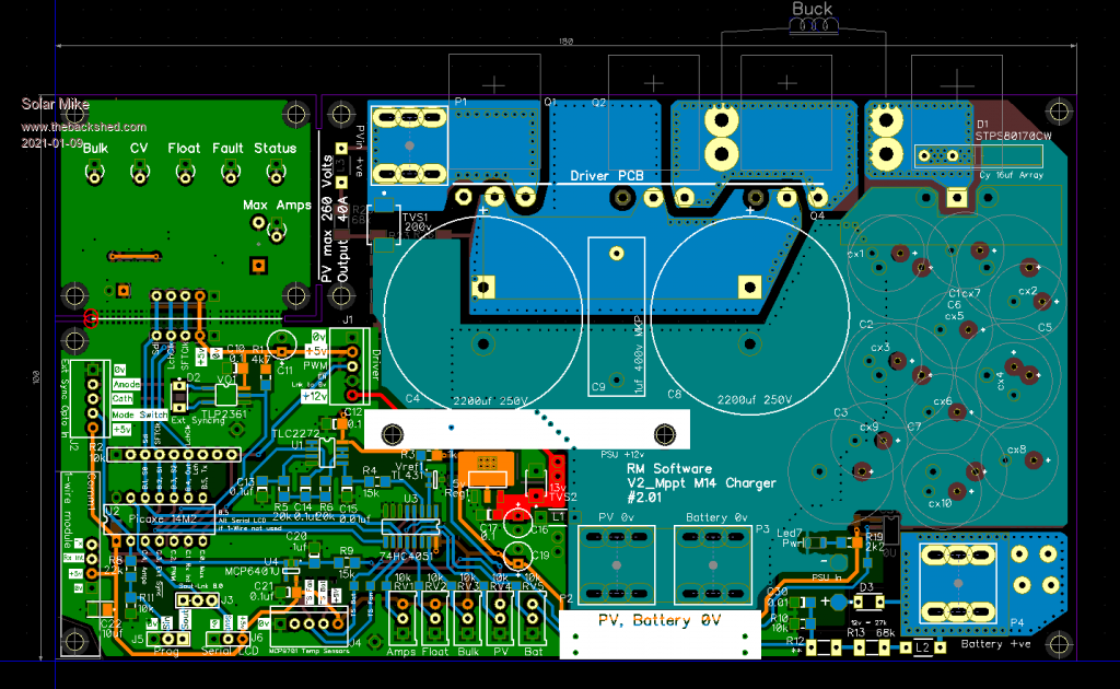
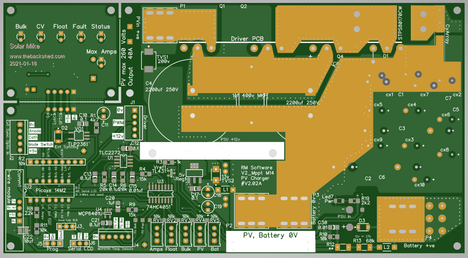
This is an updated bigger brother variation of the 08M2 design; after starting the build of the older 14M2 version, decided to augment it for a higher current and voltage rating. Most of the circuit is the same except for an additional large low esr input capacitor, use 2 buck mosfets in parallel and allowance for various combinations of output capacitors. New specs are 40A continuous charge and input PV voltage up to 250V.
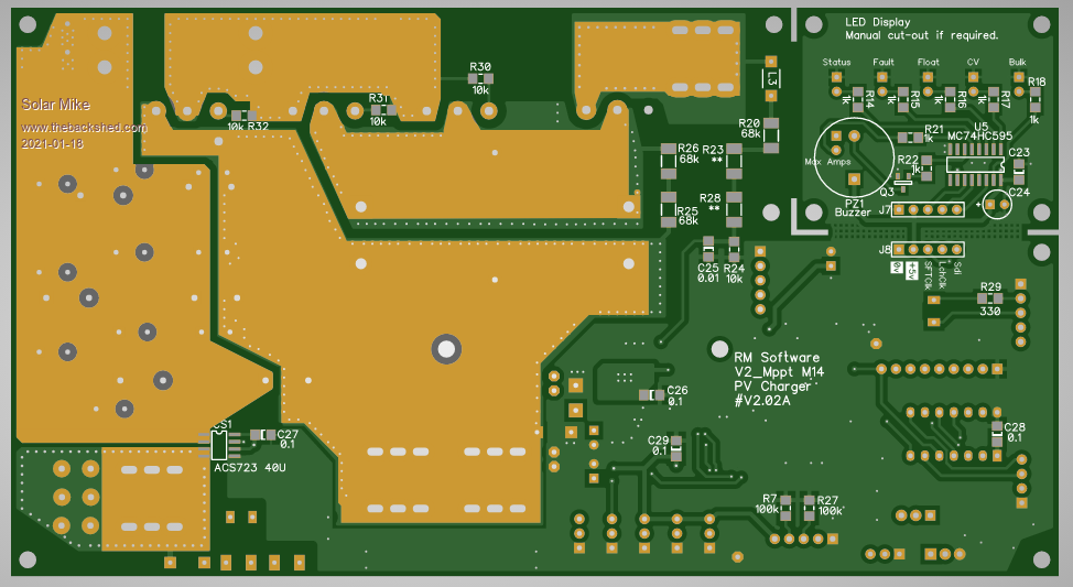
Here is the new cad layout: PCB 100 x 180mm
After building the very basic 08M2 design, decided to mount all power mosfets and dual diode off one edge of the pcb, they now sit under the pcb bolted to the alloy side panel acting as a heatsink. The mosfet driver card mounts soldered to the top mosfet pins, optimizing the drive layout and keeping all high current pcb tracks on the main pcb. Will now modify the old driver card for the additional mosfet.
Main reason for the changes are the new PV arrays that will be installed are sets of 6 x 285W panels; ie. parallel pairs of 3 series, resulting in 94Vmp at 18 amps, this will convert to approx 33 amps, 48 volt bank. The old design would just manage this but not continuously, having an extra input cap and buck mosfet allows better heat dissipation and lower losses. Track clearances have been increased to allow PV voltages up to 250V, so I can use the design on a 100V Lifepo4 bank.
Will update this thread as the design evolves.
Cheers Mike
sPuDd Senior Member Joined: 10/07/2007 Location: AustraliaPosts: 251
Posted: 11:22am 10 Jan 2021
Copy link to clipboard
Print this post
Mike,
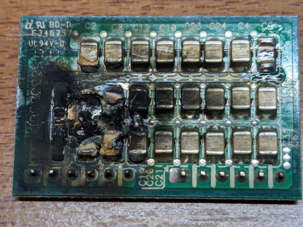
This happened to the ceramic cap low esr board on one of my MPPSolar 60amp chargers. The CCTV playback shows a wonderful shower of molten copper & lead free solder blasting out of the case bottom. I just removed the PCB, charger still works fine...
As Dave from EEVBlog has shown, the ceramics can fracture during assembly and over time which leads to catastrophic failure. I think you're mini pcb for the cap array is a good idea....
I've been following your project since last year. I'd like to assemble a few of them & test them in place of the MPPSolar ones that have been running for about two years. Looking forward to getting some boards made when you're ready.
Judd.. It should work ...in theory
Solar Mike Guru Joined: 08/02/2015 Location: New ZealandPosts: 1162
Posted: 07:36pm 10 Jan 2021
Copy link to clipboard
Print this post
Ouch, the very reason I don't use those ceramics on the main pcb in high power situations, when they blow up, they turn to carbon and arc their way though the board wrecking it.
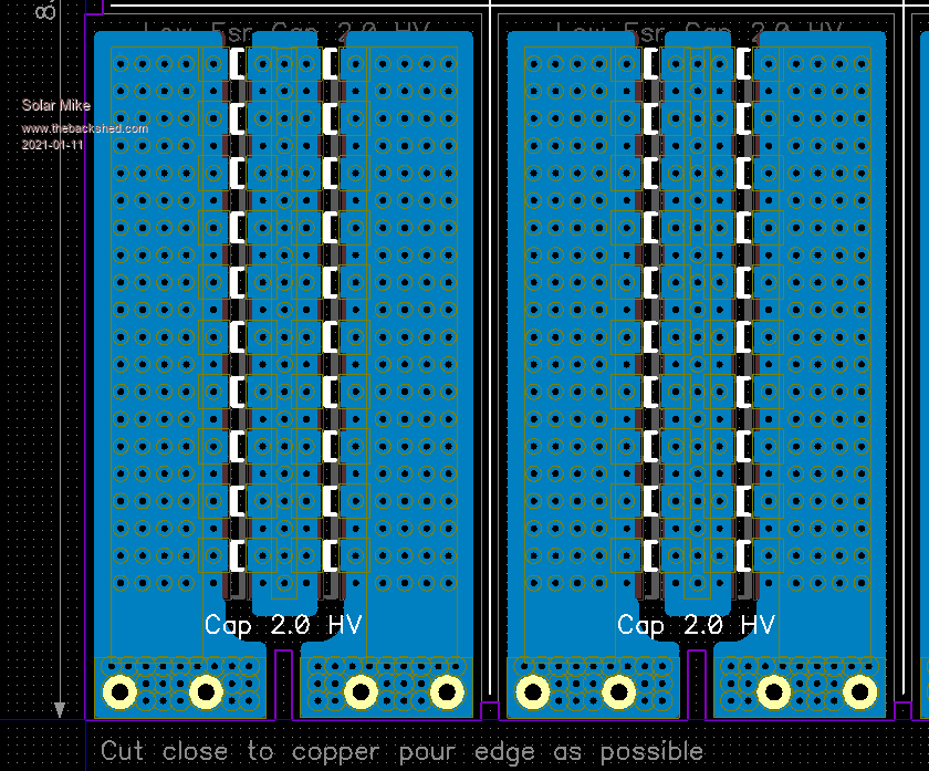
Here is the current layout showing 2 pcb's for the low esr array as used on the charger boards; note the pairs of 100V caps are in series to mitigate such disasters.
Cheers Mike
mab1 Senior Member Joined: 10/02/2015 Location: United KingdomPosts: 242
Posted: 08:12pm 10 Jan 2021
Copy link to clipboard
Print this post
Hi Mike, Thanks for sharing your PICAXE MPPT controllers - I'm planning on making 1 or a few soon.
I was looking at your PCB design above and couldn't work out how the 'freewheel' rectifier was connected up? I was expecting it to go from GND up to the FET source/inductor connection but it doesn't appear to - Am I mis-reading the board layout or have I actually spotted an error (probably the former).
Thx Marcus
nickskethisniks Guru Joined: 17/10/2017 Location: BelgiumPosts: 462
Posted: 08:44pm 10 Jan 2021
Copy link to clipboard
Print this post
Maybe a 4 layer design? Are you using synchronous rectification + an extra output series diode? Thanks for posting the design.
Would series resistors over those ceramics not help in balancing the voltages?
Solar Mike Guru Joined: 08/02/2015 Location: New ZealandPosts: 1162
Posted: 09:58pm 10 Jan 2021
Copy link to clipboard
Print this post
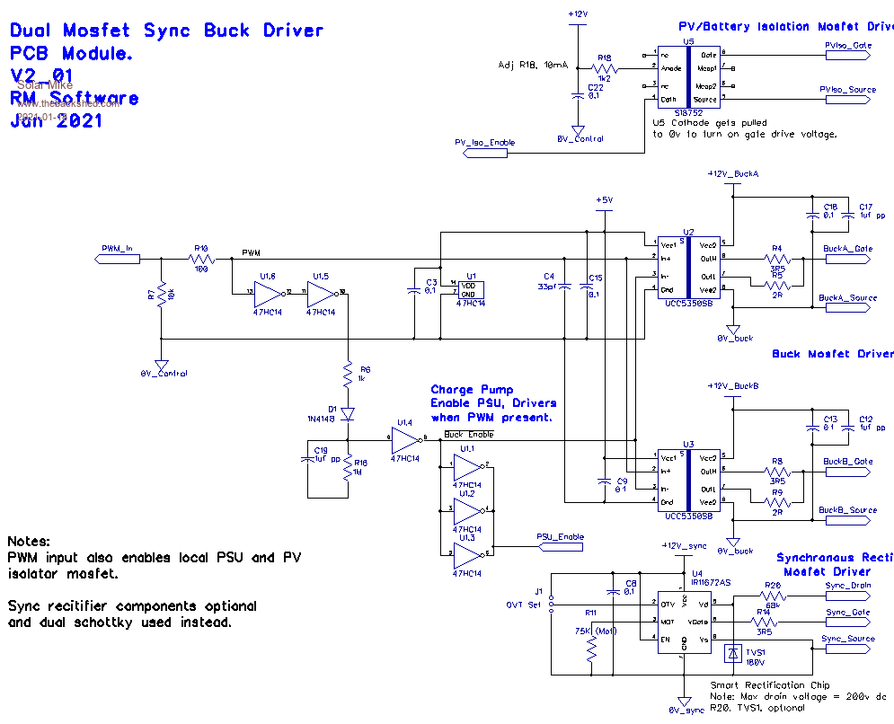
Well spotted, that layout is an early one and has the error you described, will post final layouts + driver pcb next couple of days. May modify further to allow a synchronous driver mosfet (optional).
Cheers Mike
mab1 Senior Member Joined: 10/02/2015 Location: United KingdomPosts: 242
Posted: 12:37am 13 Jan 2021
Copy link to clipboard
Print this post
Ah good, my circuit reading skills are vindicated - I like to understand how these things work even if i lack the skills to actually design one.
Solar Mike Guru Joined: 08/02/2015 Location: New ZealandPosts: 1162
Posted: 12:25am 18 Jan 2021
Copy link to clipboard
Print this post
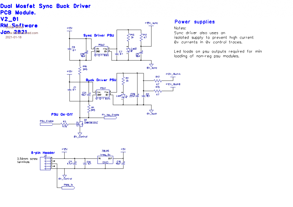
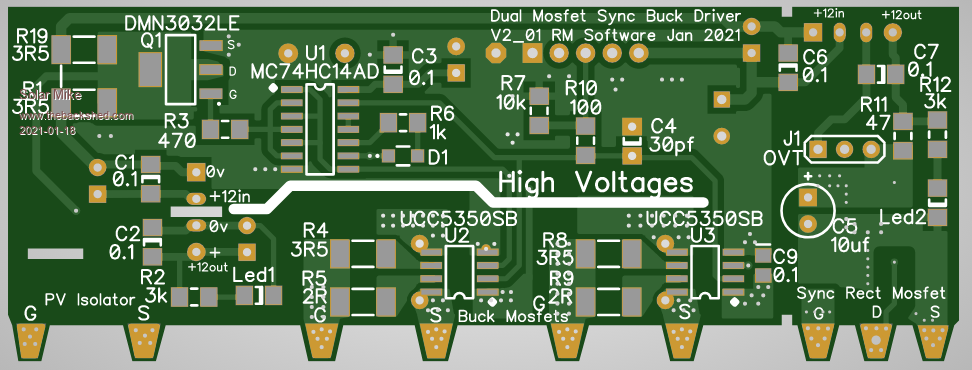
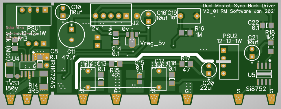
Update, here is the driver pcb that sits on top of the main pcb mosfet pads, optional components added for mosfet synchronous rectification. PCB size is 91mm x 34mm
Working on last additions to main pcb now.
Cheers Mike
Solar Mike Guru Joined: 08/02/2015 Location: New ZealandPosts: 1162