
|
|
Forum Index : Microcontroller and PC projects : PCBGOGO
| Author | Message | ||||
| CYBERLAB Newbie Joined: 08/08/2017 Location: MexicoPosts: 26 |
Hello everyone, I think several people in this forum use the company pcbgogo for the manufacture of printed circuits and apparently their costs are very cheap and their service very fast, I need to design some pcbs and I will use sprintlayout 6.0 some information that can give me about? as for example what kind of files do I have to send? someone who can provide me with an example of a design with sprintlayout that they have sent to this company to see what I have to send, thank you in advance for your help. |
||||
Grogster Admin Group Joined: 31/12/2012 Location: New ZealandPosts: 9933 |
I use GOGO and Sprint Layout 6 for all my PCB work.  Like any other PCB design software, you need to send GOGO a full set of Gerber files - one file for each layer of the board. For a double-sided board, this usually results in eight files: Top Copper, Top Silkscreen, Top Soldermask, Bottom Copper, Bottom Silkscreen, Bottom Soldermask, Board Outline and the last file is the drill data for all the holes. In Sprint Layout 6, you do this via FILE/EXPORT/GERBER EXPORT. 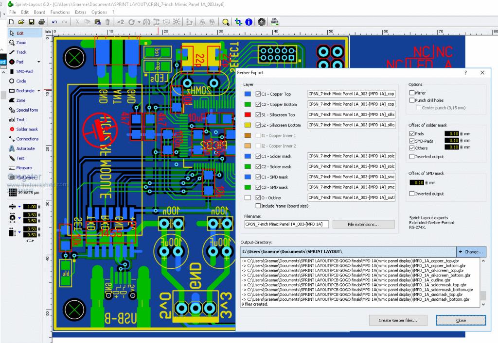 I select 0.1mm for the soldermask and SMD offset. In my case, I export two additional files, which are the SMD masks for the top and bottom SMD parts just in case the factory need them. To export the drill data, go to FILE/EXPORT/DRILL DATA, and click OK. Most PCB houses use 2,4 Inch format. 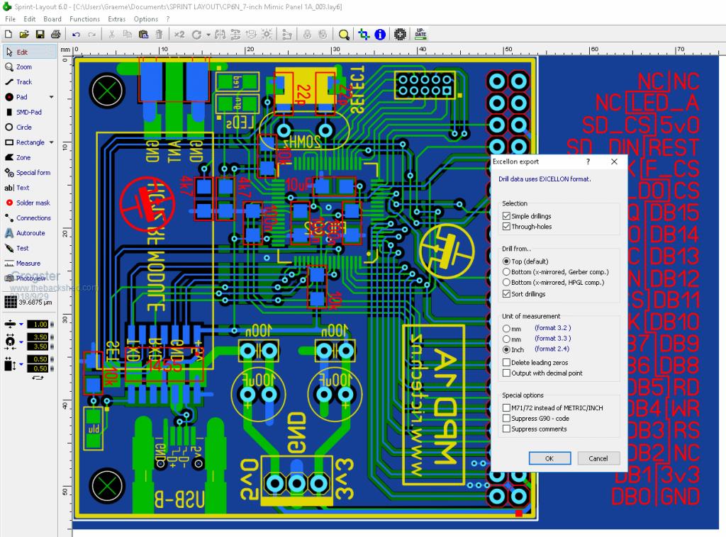 That done, look in the folder you saved your files, and use something like 7zip(google for it if you need it) to zip all the files into a single ZIP file. This single file containing all the gerber files is what you upload to GOGO or other PCB house. 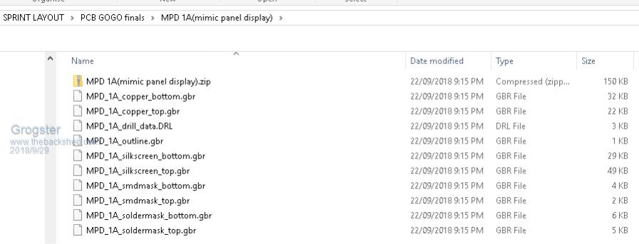 Smoke makes things work. When the smoke gets out, it stops! |
||||
Chopperp Guru Joined: 03/01/2018 Location: AustraliaPosts: 1123 |
Hey Grogs, Thanks for that info. What holes sizes do you normally use?. Components & headers etc Brian ChopperP |
||||
| Grogster Admin Group Joined: 31/12/2012 Location: New ZealandPosts: 9933 |
Square pin-headers, or polarised headers on 2.54mm spacing, I use a 2mm pad size, with a 1mm hole. For box-headers, I use 1.8mm pad, 1mm hole. For standard passives like resistors and caps etc, I use 1.8mm pad, 0.8mm hole. For 1A diodes, I use 2.2mm pad, 1mm hole. For 20x2 headers I use 1.8mm pads, 0.9mm hole. For PCB screw type terminal blocks(10mm in size, 5.08mm pin spacing) I use 3mm pad, 1.4mm hole. I have a whole HEAP of macros I have designed for various things in Sprint Layout. If any members are interested in this library, I can upload it or link to it. There are currently 298 extra parts in my personal library, which covers just about all the other parts not in the standard Sprint Layout library, including HC-12 footprints and other RF modules, DIN sockets, relays, battery holders, SPI and Parallel LCD modules, Antennas, SMA sockets, regulator modules, QFN and QFP/TQFP footprints, RTC modules, SOIC footprints, SSOP footprints, SD card sockets, Various symbols, Tact Switches, Transformers, USB sockets and Xbee modules. Smoke makes things work. When the smoke gets out, it stops! |
||||
| PeterB Guru Joined: 05/02/2015 Location: AustraliaPosts: 667 |
G'Day All Thanks Grogster for that. I had my first board done recently via FreePcb. I went into it thinking "this will never work" but it did. They are very tolerant, friendly, helpful you name it. The point is, do not be afraid! If I can do it, any idiot can. Peter |
||||
| Chopperp Guru Joined: 03/01/2018 Location: AustraliaPosts: 1123 |
Yeh, thanks Grogs. Very helpful Have things gone metric now? ChopperP |
||||
| CYBERLAB Newbie Joined: 08/08/2017 Location: MexicoPosts: 26 |
Hello again everyone, thank you very much Grogster for the information quite clear and precise, I do not think I have a problem to finish my pcbs. Thanks again for sharing! |
||||
| CYBERLAB Newbie Joined: 08/08/2017 Location: MexicoPosts: 26 |
hello Grogster, sorry what is the minimum size of pads and lines that accept in PCGOGO? |
||||
| Grogster Admin Group Joined: 31/12/2012 Location: New ZealandPosts: 9933 |
Hi. You can find that on their site, but here is a link to it: PCB GOGO CAPABILITIES Smoke makes things work. When the smoke gets out, it stops! |
||||
| The Back Shed's forum code is written, and hosted, in Australia. | © JAQ Software 2026 |
