
|
|
Forum Index : Microcontroller and PC projects : PS2 on Pico pi
| Author | Message | ||||
bigmik Guru Joined: 20/06/2011 Location: AustraliaPosts: 2981 |
Hi All, This is a 2 point question. I have little (read that as none) experience with mosfets. I see the recommended circuit for the PS2 kb on PicoMite has 2 x mosfets as level translators Actually 3 point which side is drain which side is Source on the mosfets in the example in the picoVGA manual (I told you I know nothing about mosfets) 1. Is the PS2 protocol between the PicoMite and the kb bi-directional ? (I have it somewhere in my head that the pc also talks to the kb for some reason before the kb talks to the pc) 2. IF it is mono directional, ie kb to PicoMite only, has anyone tried a using simple resistor (say 1k) in series with the kb and the GPIO pin and then a schottkey diode between the input GPIO pin and 3v3? This would clamp any voltage above say 3.5-3.6 volts on the pin. . I will attempt to test all this tomorrow but I was wondering anyone else has walked this path before me. Regards, Mick Mick's uMite Stuff can be found >>> HERE (Kindly hosted by Dontronics) <<< |
||||
| matherp Guru Joined: 11/12/2012 Location: United KingdomPosts: 11303 |
PS2 is bi-directional |
||||
| Mixtel90 Guru Joined: 05/10/2019 Location: United KingdomPosts: 8815 |
The little mosfet circuit is very neat and is bi-directional (as is PS/2). I've also tried a series resistor and schottky diode up to 3V3. It works, but you are getting close to the absolute max on the Pico pin. The series resistor has to be low enough to allow the Pico to pull down the TTL input (which may have an unknown pullup in the keyboard) yet high enough not to put too much current from a high TTL signal back to the Pico. It's not ideal. I'm not sure which picture you are looking at in the manual - the current one doesn't seem to have that picture. However, the Source is towards the PicoMite site (with a pullup to 3V3) and the Drain is towards the keyboard side (with a pullup to 5V). The Gate is connected directly to 3V3. This is an N-channel mosfet. Edited 2022-06-08 20:23 by Mixtel90 Mick Zilog Inside! nascom.info for Nascom & Gemini Preliminary MMBasic docs & my PCB designs |
||||
| bigmik Guru Joined: 20/06/2011 Location: AustraliaPosts: 2981 |
Wow blokes, Thank you for the quick responses, Ok now that I know it IS bi-directional I think I MUST use the mosfet circuit. That leaves just the question as to which pin is S(ource) and which is D(rain) in this schematic ? 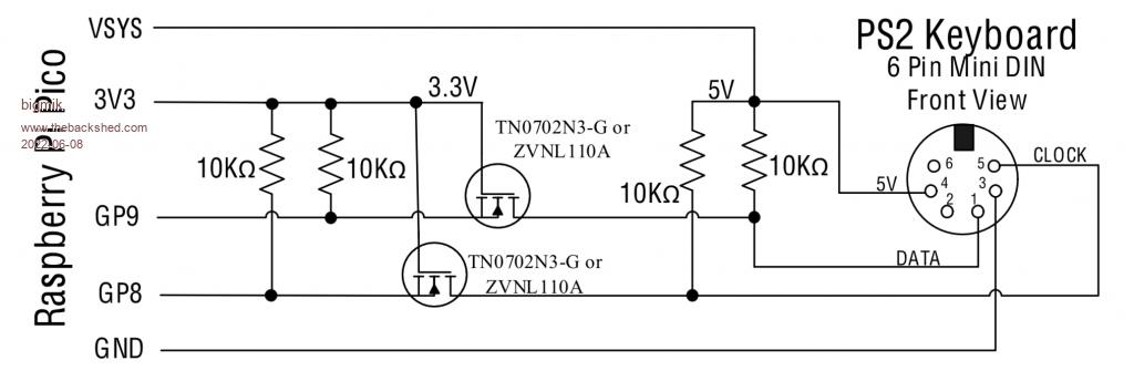 I assume the top pin is the G(ate) as it looks the same in just about every mosfet diagram I see. I think the Source is the PicoMite side and Drain the kb side but I don�t want my valuable pS2 keyboard to do a �Cheech and Chong� Regards, Mick Mick's uMite Stuff can be found >>> HERE (Kindly hosted by Dontronics) <<< |
||||
| matherp Guru Joined: 11/12/2012 Location: United KingdomPosts: 11303 |
The design authority Edited 2022-06-08 20:34 by matherp |
||||
| bigmik Guru Joined: 20/06/2011 Location: AustraliaPosts: 2981 |
Thank you Peter, That shows my assumption was actually correct. That link looks like a very interesting read, I will see if this old dog can learn some new tricks by reading through it in its entirety. Thank you again for your never ending work on porting to different devices, the Pico-Pi has perked me out of the doldrums and gotten me back in the hardware again. I just love that little beastie. Kind Regards, Mick Mick's uMite Stuff can be found >>> HERE (Kindly hosted by Dontronics) <<< |
||||
| phil99 Guru Joined: 11/02/2018 Location: AustraliaPosts: 3188 |
The main reason it is important to get drain and source the right way around is that there is a diode between drain and source (also missing from that diagram along with the pin labels) with anode to source (Pico side) and cathode to drain (KB side). Get it wrong and you have 4.4V on the Pico pin. Fully bi-directional MOSFETS without the diode do exist but are as common as hens teeth. The diode results from the fabrication process, eliminating it requires several more expensive processing steps. Those ones are a bit like the symmetrical bipolar transistors that once existed, interchangeable emitter and collector. Edited 2022-06-09 11:03 by phil99 |
||||
Grogster Admin Group Joined: 31/12/2012 Location: New ZealandPosts: 9954 |
Mick - I'm very much like you, in that when I did my servicing training, everything(pretty much) was bi-polar transistors in the NPN or PNP flavours. When I was doing my apprenticeship, I remember needing to have those big, fat, transistor equivalents books on my desk, so I could look up a suitable replacement for transistor X that had just blown itself to bits, but I could not get the exact replacement for a repair.  I came across the OCCASIOAL rouge FET or JFET, but most stuff was transistor. I never really played with MOSFET's at all, till I started tinkering with BASIC stamp, then PICAXE, now Micromite series. The key thing to remember with MOSFETS that helped me remember how they work and why, is that they are a VOLTAGE-DRIVEN device. As you will know well, in an NPN for example, the C-E current is controlled by the current flowing in the B-E path. With a MOSFET, the S-D current is controlled by the VOLTAGE potential on the gate. This is what makes them so fan-diddly-tastic on MCU's like the Micromites etc, as the gate current is effectively zero, so you can drive them beautifully with just an I/O pin, even if that pin can only sink or source 10mA or less. Some bipolar's would need more then that to drive them to saturation, so you end up having to use Darlington arrangements to get enough oomph out of them. That, and most MOSFET's have an exceptionally low S-D resistance when fully on, so they dissipate considerably less heat then bipolar transistors at the same voltage and current. That's when they are fully on. A MOSFET can dissipate a HUGE amount of heat if you DON'T drive it fully into saturation, and that is one thing that can kill MOSFETS, as half-on MOSFETS with a reasonable voltage and current behind them, can turn into little nuclear reactors if you let them!  MOSFET's are also considered to be static-sensitive, especially where the gate pin is concerned, and many of them can be killed by static discharge into the gate, so they need more TLC then your average bipolar that you can drop-kick from the car to your workshop and they will still work fine.  This is a very simple description just to help you on your way with MOSFET's, but once you discover how brilliant they can be, you'll probably never want to use a bipolar transistor again in your designs, unless for some reason, you HAVE to. Smoke makes things work. When the smoke gets out, it stops! |
||||
| Mixtel90 Guru Joined: 05/10/2019 Location: United KingdomPosts: 8815 |
MOSFETS actually have more in common with triode valves than they do with bipolar transistors. Even their gate voltage - drain current curve shapes are similar in some cases. Like valves they are pretty awful for power dissipation when run in the linear part of their curve. Mick Zilog Inside! nascom.info for Nascom & Gemini Preliminary MMBasic docs & my PCB designs |
||||
| bigmik Guru Joined: 20/06/2011 Location: AustraliaPosts: 2981 |
Thank you All, When I started my electronics course nearly 50 years ago I started learning valves as well as transistors. I now remember nothing about my valve training and a lot of my transistor knowledge has gone astray as well. I have ordered some of every variety of mosfets recommended by those in the know in one of my previous posts so when they arrive I can do some experiments (and no doubt smoke letting) Regards, Mick Mick's uMite Stuff can be found >>> HERE (Kindly hosted by Dontronics) <<< |
||||
| The Back Shed's forum code is written, and hosted, in Australia. | © JAQ Software 2026 |
