
|
|
Forum Index : Microcontroller and PC projects : PicoMite RP2350B DIL Development board, 16Mb flash + 8 MB PSRAM
| Author | Message | ||||
| toml_12953 Guru Joined: 13/02/2015 Location: United StatesPosts: 655 |
I just ordered 5 of these. I only need one so if anyone in the US or Canada needs one, I'd sell it for $25.00, including shipping. It may sound expensive but it's cheaper than ordering the minimum from JLC. Oh, BTW, I'll include the two 32-pin headers but you'll have to solder them on yourself. |
||||
| circuit Guru Joined: 10/01/2016 Location: United KingdomPosts: 305 |
I rather lost the plot on this one; I caught a rather bad dose of Covid shortly after my original post and that took me out of a lot of activities for a surprisingly long time. Surprising because I had had every available dose of vaccine provided by the NHS. Anyway, I am now fully back on my feet and catching up with life in a wide range of activities. Firstly, here is a corrected form of the original image: 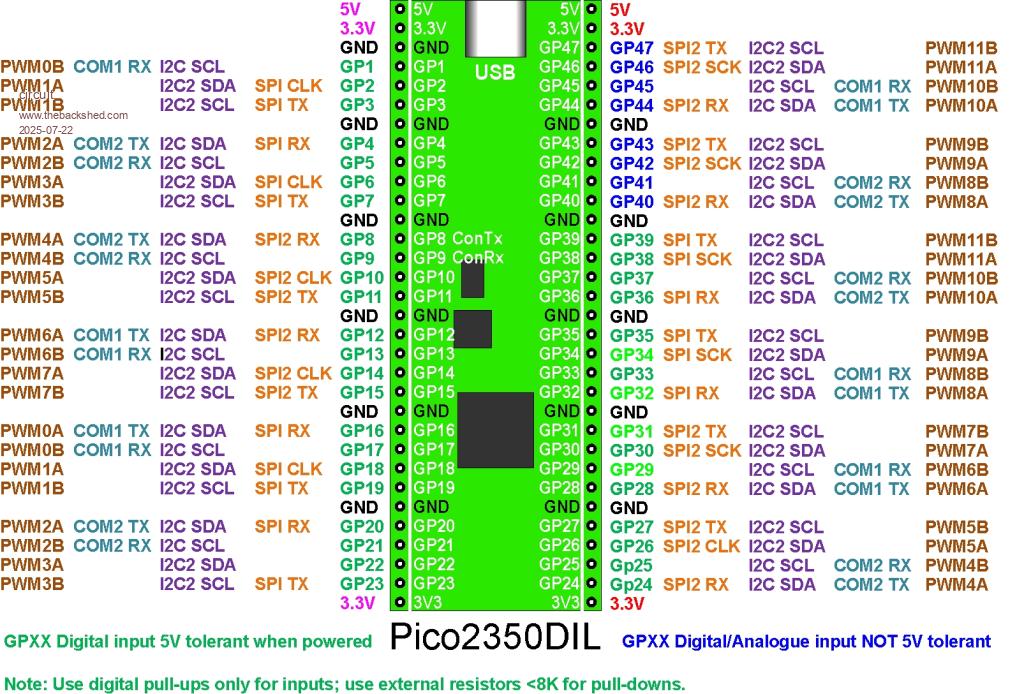 As for a high resolution version, I have not tried this before, but here is a .PDF upload; Pico2350DIL - Peter Mather Design.pdf |
||||
| PhenixRising Guru Joined: 07/11/2023 Location: United KingdomPosts: 1954 |
PDF is great, many thanks  |
||||
| circuit Guru Joined: 10/01/2016 Location: United KingdomPosts: 305 |
May I ask for some advice, please, on power supplies. The original Pi Pico boasts a "flexible power system (ref Picomite Manual)". This buck-boost SMPS supply allows an input voltage of 1.8 to 5.5 volts and the VSYS pin is connected to the VBUS and USB input through a diode. I use Picomites for embedded control and therefore I normally connect in my external 5.0 v. supply to the VSYS pin via a Schottky diode. (In fact, given that the SMPS supply will work right down to 1.8 volts, I normally just use a 1N4002 diode as the forward voltage drop will make little difference to the buck-boost unit. This works brilliantly, giving me plenty of horsepower for my peripheral chips. My problem is, how does all this translate to the Pico2350DIL. I need to power it externally through the 5 volt pins and to simultaneously connect the USB for programming. I thought to put a diode between my 5 volt supply and the feed to the whole circuit, (Pico2350DIL+various interface chips and 5v IRLED relays etc) but given the not quite so favourable drop-out voltage of the AMS117 at a possible 1.3 volts, there is virtually no headroom over the diode forward voltage drop (and I cannot seem to make out if there is a diode protection on the board between the USB and the regulator). My current compromise is to load the firmware over the USB with the external 5v board supply disconnected, then to program and interact over the GP8/GP9 console connection, however, I would much prefer a configuration analogous to the standard 2040 boards. (and I would like GP8/GP9 back for other purposes). What would I be advised to do to power the Pico2350 from a 5 volt external source and still maintain a protected USB connection? Edited 2025-08-03 23:28 by circuit |
||||
| matherp Guru Joined: 11/12/2012 Location: United KingdomPosts: 11498 |
If you look at the PCB with the USB-C at the top, there is a thick track coming out from under the USB-C to the right of the connector.This then splits in two, one part leg goes to the AMS1117 and the other to the top right 5V pin. If you cut the thick track before the split it will isolate the USB supply. If you really want to be fancy you could expose the copper either side of the cut and solder on a SMD 1N5819 schottky diode - there should be just about enough space. If you haven't purchased the PCBs yet I can easily add the diode and post you some new gerbers Edited 2025-08-04 00:18 by matherp |
||||
| circuit Guru Joined: 10/01/2016 Location: United KingdomPosts: 305 |
Peter, as ever, thank you. Scalpel at the ready, 2350DIL now under the microscope and about to sever the artery. I haven't got any 5819s in stock, but they are now in my Mouser basket ready for implantation later in the week! |
||||
| PhenixRising Guru Joined: 07/11/2023 Location: United KingdomPosts: 1954 |
What I did was make up a USB cable, sans 5v wire. |
||||
Bryan1 Guru Joined: 22/02/2006 Location: AustraliaPosts: 2092 |
Well time to bump this thread as it is a good reference  With my cnc going down one job was in my mind was this board as I did buy all the gear back in the day. So used that brandnew breadboard and soldered setup the board then soldered all the pins, also got a couple of USB2 breakout boards and a few SDCard breakout boards. Had search back to last year and the first thing I did was printout that picture and printed it on my colour laser printer. So now got research where everything goes and get it all connected and going as I am thinking of setting up the stepper code so I can test this X axis stepper and see if it is the problem. Regards Bryan |
||||
| BarryH Regular Member Joined: 05/01/2025 Location: AustraliaPosts: 45 |
After recently working on the PICO2350DIL module away from my usual environment, and not have my usual resources, I was a bit stuck on some development as I couldn't correlate pins to GP numbers. LIST PINS and MM.INFO(PINNO GPnn) report incorrect mappings, and a back shed reply indicated this is because the pins above GP28 have "virtual" pin numbers that don't reflect any specific layout. The firmware can't know what variant of PCB a RP2350B is on, and there isn't a Raspberry Pi standard for the RP2350B. To mitigate this experience in the future, I have developed "PICO2350DIL Help.txt" help file. Copy to your a: drive and rename to help.txt for keyword searches, or keep as is on any drive and list within the file manager. Pico2350DIL Help File.zip BarryH |
||||
| Mixtel90 Guru Joined: 05/10/2019 Location: United KingdomPosts: 8903 |
The golden rule is to *NEVER EVER* use or rely on board pin numbers in any way whatsoever, even if it involves additional programming, documentation and writing comment lines in your program to explain why you have done it. The RPnnnn uses the GPnn numbers internally so those are always correct. All PCB pin numbers are meaningless. Mick Zilog Inside! nascom.info for Nascom & Gemini Preliminary MMBasic docs & my PCB designs |
||||
| BarryH Regular Member Joined: 05/01/2025 Location: AustraliaPosts: 45 |
Absolutely agree and know the value of only using GP numbers in code, however pin numbers are not entirely useless. If the module doesn't have a screen print of the GP numbers, or you don't have easy access to to the screen print, then at some stage you will be counting the physical pins of a module to make connections. BarryH |
||||
| Plasmamac Guru Joined: 31/01/2019 Location: GermanyPosts: 620 |
Because i need do give up my sheed/home i cant find a lot from my mmbasic devices. Most of them are throw away but its ok . Friends clear my home and have no clue about my hobbys. If anyone can send me the latest device from peter so chime in here. Because the expansive postage i prefere german users. My incoming from german krankenkasse need time Plasma |
||||
| Plasmamac Guru Joined: 31/01/2019 Location: GermanyPosts: 620 |
I‘ll will pay for Plasma |
||||
| matherp Guru Joined: 11/12/2012 Location: United KingdomPosts: 11498 |
I'd be happy to send you one, no charge, but I won't be at home in the UK for a couple of weeks Edited 2026-05-19 01:21 by matherp |
||||
| Plasmamac Guru Joined: 31/01/2019 Location: GermanyPosts: 620 |
Great , thx Plasma |
||||
| The Back Shed's forum code is written, and hosted, in Australia. | © JAQ Software 2026 |
