
|
|
Forum Index : Microcontroller and PC projects : how do connect the ps/2 keyboard connector to this 2N700
| Author | Message | ||||
| tenij000 Senior Member Joined: 30/05/2025 Location: NetherlandsPosts: 107 |
dont now how this 2N700 is connected 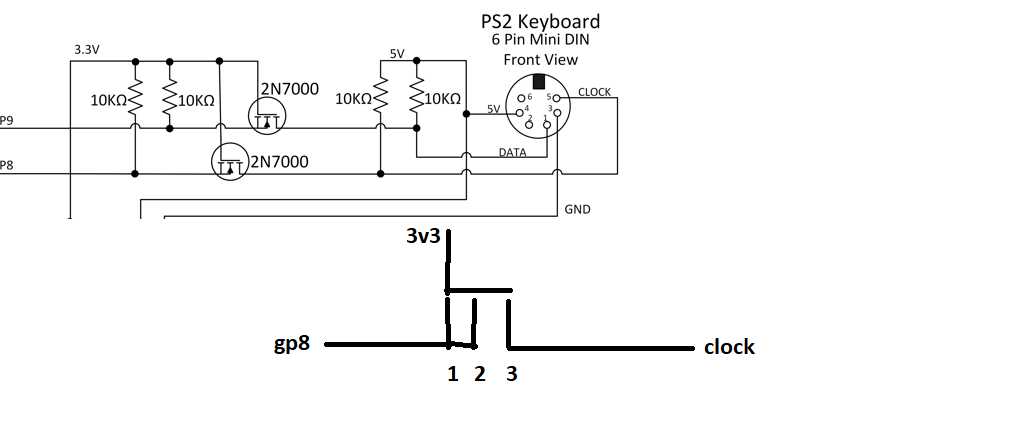 3v3 connected to pin 3 ? gp8 connected to pin 1 and 2 pin 3 connected clock |
||||
| Mixtel90 Guru Joined: 05/10/2019 Location: United KingdomPosts: 8911 |
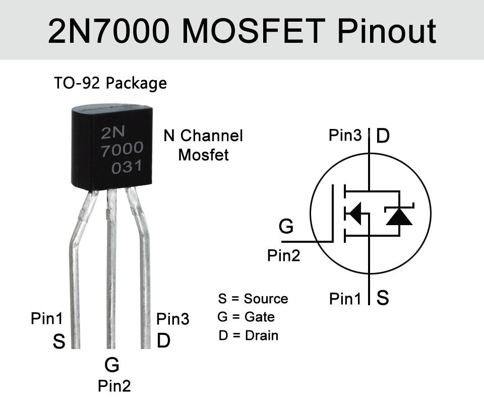
How do you mean? That's a conventional level shifter circuit using a common N-channel mosfet. GP8 - source - pin 1 3V3 - gate - pin 2 PS2 CLK - drain - pin 3 If you look at the mosfet from the top with the flat side towards you the pins are in 1-2-3 order left to right. What you have labelled as pin 2 is wrong. On a mosfet symbol the source is indicated by both what you have labelled as pin 1 and the centre line with the arrow on it. The direction of the arrow shows weather it is N-channel )towards the gate) or P-channel (away from the gate). Mick Zilog Inside! nascom.info for Nascom & Gemini Preliminary MMBasic docs & my PCB designs |
||||
| javavi Guru Joined: 01/10/2023 Location: UkrainePosts: 562 |
 3v3 connected to pin 2 - GATE GP8 connected to pin 1 - SOURCE CLOCK connected to pin 3 - DRAIN Edited 2025-07-17 20:32 by javavi |
||||
| tenij000 Senior Member Joined: 30/05/2025 Location: NetherlandsPosts: 107 |
like this 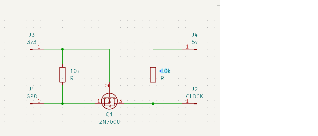 |
||||
| stanleyella Guru Joined: 25/06/2022 Location: United KingdomPosts: 2807 |
https://nl.aliexpress.com/item/32890488553.html? |
||||
| EDNEDN Senior Member Joined: 18/02/2023 Location: United StatesPosts: 295 |
I have used these exact modules a number of times. They work well, but they do delay the signal noticeably. I had the clock not routed though the converter but the data was routed through the converter. And I could not reliably latch the data. |
||||
| phil99 Guru Joined: 11/02/2018 Location: AustraliaPosts: 3293 |
The 10kΩ pullups are a bit high for speed. On the 3.3V side 1.8kΩ and 2.7kΩ on the 5V side would be better. If that still isn't enough 680Ω and 1kΩ are as low as I would go. |
||||
| Mixtel90 Guru Joined: 05/10/2019 Location: United KingdomPosts: 8911 |
Connecting one line via a mosfet and the other not is exactly like adding a capacitor to one of the signals. You can expect the signal to be delayed - that's how mosfets work. :) If the clock speed is reasonable then putting both clock and data via mosfets works fine as the signals remain in synch. 10k is ok for the pull-ups in most cases. It needs to be reduced at higher frequencies to charge the capacitors in the mosfets (and any signal line capacitance) quicker, but at PS2 speeds it's ok. Mick Zilog Inside! nascom.info for Nascom & Gemini Preliminary MMBasic docs & my PCB designs |
||||
| The Back Shed's forum code is written, and hosted, in Australia. | © JAQ Software 2026 |
