
|
|
Forum Index : Microcontroller and PC projects : uMite (mx170) with USB/programmer DIP28
| Author | Message | ||||
| robert.rozee Guru Joined: 31/12/2012 Location: New ZealandPosts: 2541 |
if only they'd placed the pins on a 0.1" grid, then folks would have been able to just plug a piece of veroboard on top instead of buying expensive 'blank shields' - to my mind, this would have helped boost adoption of the full-sized arduino boards. i really can't believe that the off-grid placement of one of the connectors was an accident. i've found the nano format (and similar) to be ideal for experimenting. a quick question for MicroBlocks: why are pins 4 and 5 not brought out to the pin headers down the sides? when not using the ICSP programming these pins have normal mmbasic functions. and the two needed pads could be reclaimed by dropping "ICSP:3.3V" and "ICSP:GND" which are duplicates of "+3.3V" and "GND" respectively. cheers, rob :-) |
||||
| MicroBlocks Guru Joined: 12/05/2012 Location: ThailandPosts: 2209 |
@Rob, Yes, that would have been better. It does require a complete new routing of the board because everything needs to be shifted around. When i was made aware (by you and Mick) the files were already send. Version 2 will have them available. I used the arduino pro a lot, also a very compact format (similr as the nano) and easy to plop into a breadboard or veroboard. I think i have only one shield for an arduino uno. Did not like it and it was the last i used a uno. I think the 'mistake' was a move made deliberatly to create a specific market. Microblocks. Build with logic. |
||||
| panky Guru Joined: 02/10/2012 Location: AustraliaPosts: 1130 |
@MicroBlocks Jean, No problems using the pin layout diagram - if you need a hi res vector to use just drop me a PM with your email address (same for anyone else wanting to use the artwork) Great little module - I am particularly interested in the 44 pin little rascal when you get it done. 
Cheers, Doug. ... almost all of the Maximites, the MicromMites, the MM Extremes, the ArmMites, the PicoMite and loving it! |
||||
| MicroBlocks Guru Joined: 12/05/2012 Location: ThailandPosts: 2209 |
Thanks Panky! After a good nights sleep i woke up with the solution to include pin 4 and 5. So the new layout is: 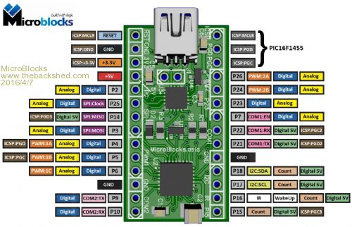
An updated full size version is on github:UMX170 Pinout Just moved the pcb's to the lowest drawer, as this one is better and the best is what i want. I will do a new round of double checking all connections before sending the files. Not really want to have another 200 pcb's going to waste. Microblocks. Build with logic. |
||||
| robert.rozee Guru Joined: 31/12/2012 Location: New ZealandPosts: 2541 |
looking at your revised supervisory circuit, i suspect R1 can be shorted out and that R2 is not needed. any chance you could post a revised schematic for comment? i very much like the new pinout. cheers, rob :-) |
||||
| MicroBlocks Guru Joined: 12/05/2012 Location: ThailandPosts: 2209 |
The pinout on github is correct, the one on this forum i could not update anymore. The reset pin now goes directly to the mclr on the mcu. The supervisory chip is used in a standard way. I also added pin numbers to the silkscreen to make it more clearer when only using the pcb. 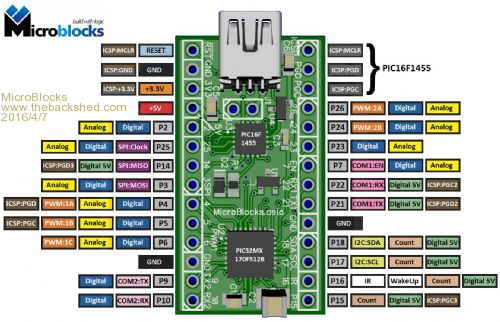
UMX170 Pinout Schematics One thing still to do and that is to add a header for a reset/gnd/+3v and switch the pins for reset and GND to bring it in line with the other module (UMX170-44) Microblocks. Build with logic. |
||||
| robert.rozee Guru Joined: 31/12/2012 Location: New ZealandPosts: 2541 |
have you considered using the SOT-89 version of the MCP1700? this would give you some extra thermal headroom in case of the micromite driving significant loads. also, could J1 be replaced with a schottky diode, eliminating the board space consumed by the jumper. cheers, rob :-) |
||||
| MicroBlocks Guru Joined: 12/05/2012 Location: ThailandPosts: 2209 |
The 'jumper' is so that the user can choose if they want a jumper, PTC or a ... diode. :) It can also serve as an connection to measure current (high side). I have a bunch of traces on the bottom side that prevent placement of a SOT-89 version. I can have a look if they can be moved to make room. Microblocks. Build with logic. |
||||
| robert.rozee Guru Joined: 31/12/2012 Location: New ZealandPosts: 2541 |
you could place the voltage regulator on the underside perhaps? do you have a reverse-side image? i presume the pcb is only 2-layers. cheers, rob :-) |
||||
| MicroBlocks Guru Joined: 12/05/2012 Location: ThailandPosts: 2209 |
I would prefer only topside and surface mounted as they can be processed in a single reflow. I have placed larger solder areas under the regulator and added vias to increase the heat dissipation. 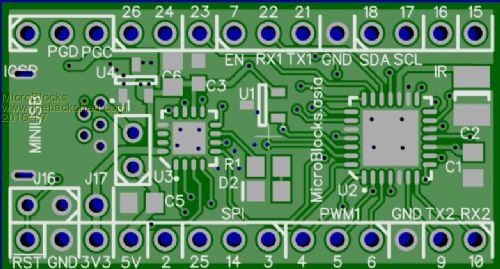
This is from the datasheet of the MCP1700 POWER DISSIPATION EXAMPLE Package Package Type = SOT-23 Input Voltage VIN = 2.3V to 3.2V LDO Output Voltages and Currents VOUT = 1.8V IOUT = 150 mA Maximum Ambient Temperature TA(MAX) = +40�XC Internal Power Dissipation Internal Power dissipation is the product of the LDO output current times the voltage across the LDO (VIN to VOUT). PLDO(MAX) = (VIN(MAX) - VOUT(MIN))xIOUT(MAX) PLDO = (3.2V - (0.97 x 1.8V)) x 150 mA PLDO = 218.1 milli-Watts The specific packages: Maximum Package Power Dissipation at +40�XC Ambient Temperature 2x2 DFN-6 (91�XC/Watt = R��JA) PD(MAX) = (125�XC - 40�XC) / 91�XC/W PD(MAX) = 934 milli-Watts SOT-23 (230.0�XC/Watt = R��JA) PD(MAX) = (125�XC - 40�XC) / 230�XC/W PD(MAX) = 369.6 milli-Watts SOT-89 (52�XC/Watt = R��JA) PD(MAX) = (125�XC - 40�XC) / 52�XC/W PD(MAX) = 1.635 Watts TO-92 (131.9�XC/Watt = R��JA) PD(MAX) = (125�XC - 40�XC) / 131.9�XC/W PD(MAX) = 644 milli-Watts Worst case would be a 5v supply and 250ma current. PLDO = (5V - (0.97 x 3.3V)) x 250 mA PLDO = 449.75 milli-Watts Using the above it would seem that a save amount of current is around 200ma. Microblocks. Build with logic. |
||||
| MicroBlocks Guru Joined: 12/05/2012 Location: ThailandPosts: 2209 |
Updated the silkscreen. Added two pins to access the console. Added two fiducials to help with P&P. Still pondering over the regulator. 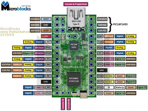
Highres on github: UMX170 Pinout Microblocks. Build with logic. |
||||
| robert.rozee Guru Joined: 31/12/2012 Location: New ZealandPosts: 2541 |
why have you duplicated RESET, GND and +3.3V connections? normally these would be carried through to a carrier board anyway (where the reset switch would be located). good idea exposing in particular CTX, as in some aplications this may be connected to WAKEUP. cheers, rob :-) |
||||
| MicroBlocks Guru Joined: 12/05/2012 Location: ThailandPosts: 2209 |
The idea (at that time) was that you could use jumpers with the pins to the top at that location to easily access them for reset and power, while all the outer pins are on the bottom. But they are not really necessary, and when dropping those i win some space for the other regulator package which would be a better use of the space. I'll give that a try. Thanks for keeping me on my toes. 
Really appreciate that as sometimes things are overlooked for a better option. Microblocks. Build with logic. |
||||
| MicroBlocks Guru Joined: 12/05/2012 Location: ThailandPosts: 2209 |
I figured out a way to get the SOT-89 version on the PCB. Moved some parts and got some room because the extra set of reset, 3.3v and 5v pins are removed. I also added a 10 ohm resistor and 100n capacitor to the AVDD and AVSS pins. These are not in the basic schematic from the uMite, but they should be there. Will update the image soon. edit: Updated image: 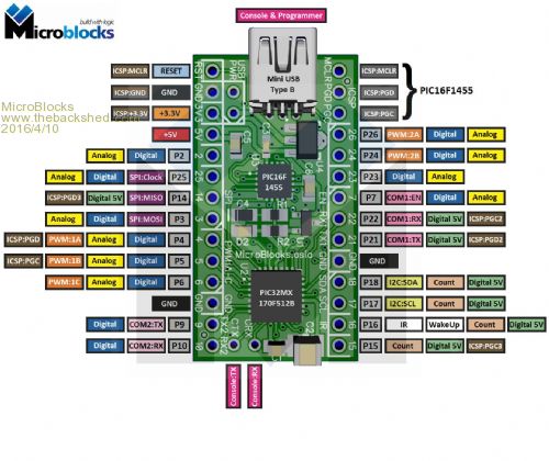
Highres on github: UMX170 Pinout Microblocks. Build with logic. |
||||
| robert.rozee Guru Joined: 31/12/2012 Location: New ZealandPosts: 2541 |
looking good |
||||
| MicroBlocks Guru Joined: 12/05/2012 Location: ThailandPosts: 2209 |
Being very busy with setting up some form of assembly the QFN's are not going to happen unfortunately. To much time with too high failure. So i am in the process to replace the QFN's with (T)SSOP packages. Surprisingly it does not take more space as the routing can be done using less vias. This because the SSOP does not have a EP on the bottom which makes putting traces under the chip impossible. 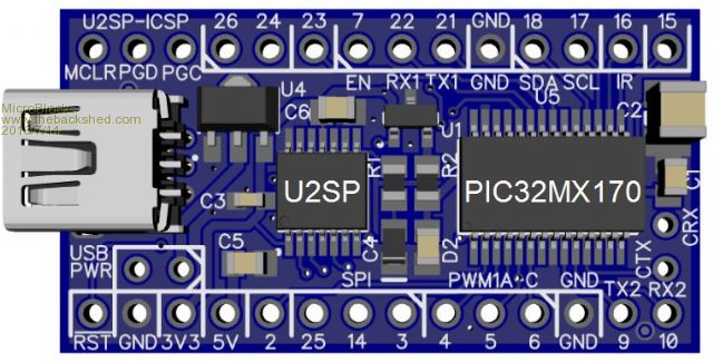
I have a few more 'blocks' to convert to SSOP and then it will be time to place an order for the PCB's and get things going. Microblocks. Build with logic. |
||||
| Zonker Guru Joined: 18/08/2012 Location: United StatesPosts: 772 |
Awesome module MB..! 
These should sell very well, as this forms a great 28 pinner start-up module to get new users going on the MM.. I still have a few of my 28 pinner modules left, and I use them often to check out new hardware tests... Lookin good boss..!! Can't wait for the production run..!! |
||||
| The Back Shed's forum code is written, and hosted, in Australia. | © JAQ Software 2026 |
