| |
  Page 2 of 2 Page 2 of 2 |
| Author |
Message |
Grogster

Admin Group

Joined: 31/12/2012
Location: New ZealandPosts: 9985 |
| Posted: 03:23pm 29 Mar 2016 |
 Copy link to clipboard Copy link to clipboard |
 Print this post |
|
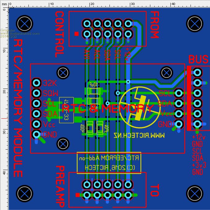
Will upload an example photo shortly, so you can see what I mean....
EDIT: OK, here is an image of my simple RTC carrier board:
Now, using photoview(down bottom of left-side menu), it will look like this from the PCB house:

Note how the three vias between layers are covered in soldermask like the rest of the board - you can't solder to these, they are covered up as they are just vias. Pads can also act as vias too, but solderable ones.
Sorry if I am confusing you - not my intention.
EDIT: Same board but with the vias NOT clicked with the mouse using the SOLDERMASK menu option on the left:
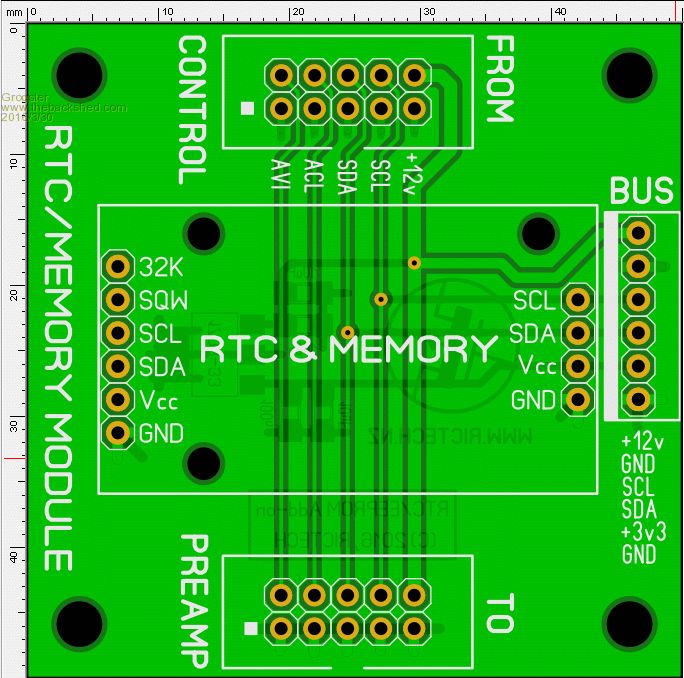
Note how these vias would show up as solderable pads from top or bottom.
There is no need for that, so I cover them all up, if you see what I mean.
There is no reason why you can't leave them all as solderable vias if you like - this is just what I like to do, but is by no means scripture.Edited by Grogster 2016-03-31
Smoke makes things work. When the smoke gets out, it stops! |
| |
Herry

Senior Member

Joined: 31/05/2014
Location: AustraliaPosts: 261 |
| Posted: 08:37am 31 Mar 2016 |
Copy link to clipboard |
Print this post |
|
Thanks. I think at this stage I'll just go for solderable vias without the mask.
Senior?! ĀWhatever it says, I'm a complete and utter beginner... |
| |
Herry
Senior Member
Joined: 31/05/2014
Location: AustraliaPosts: 261 |
| Posted: 08:38am 31 Mar 2016 |
Copy link to clipboard |
Print this post |
|
Another matter: See Gerber question in the thread 'PCB Manufacture'.
Senior?! ĀWhatever it says, I'm a complete and utter beginner... |
| |
Herry
Senior Member
Joined: 31/05/2014
Location: AustraliaPosts: 261 |
| Posted: 10:36am 01 Apr 2016 |
Copy link to clipboard |
Print this post |
|
Just in case there are people out there who are even more raw beginners at Sprint Layout (and everything else) than me, here's a tip: If it is desired to delete all connected tracks at once, use the test function and press delete when the prod has activated a particular connection.
BUT see next post!Edited by Herry 2016-04-03
Senior?! ĀWhatever it says, I'm a complete and utter beginner... |
| |
Herry
Senior Member
Joined: 31/05/2014
Location: AustraliaPosts: 261 |
| Posted: 08:47am 02 Apr 2016 |
Copy link to clipboard |
Print this post |
|
Yes... (cough) well... (further cough). That was all very well and good until I noticed that although deleting a flashing connection identified by the test prod did indeed remove all connections at once, it also removed the connected pins of whatever device it was connected to/through. So for example, I now have a DIL28-300 with missing pins! So, almost certainly a useless 'tip'!
Senior?! ĀWhatever it says, I'm a complete and utter beginner... |
| |
Herry
Senior Member
Joined: 31/05/2014
Location: AustraliaPosts: 261 |
| Posted: 03:30pm 02 Apr 2016 |
Copy link to clipboard |
Print this post |
|
Next question: When I design a board, I have no idea what dimensions it needs to be until I have placed all the components, so I cannot use New Board first. What is the way round that?
Senior?! ĀWhatever it says, I'm a complete and utter beginner... |
| |
Grogster
Admin Group
Joined: 31/12/2012
Location: New ZealandPosts: 9985 |
| Posted: 09:25pm 02 Apr 2016 |
Copy link to clipboard |
Print this post |
|
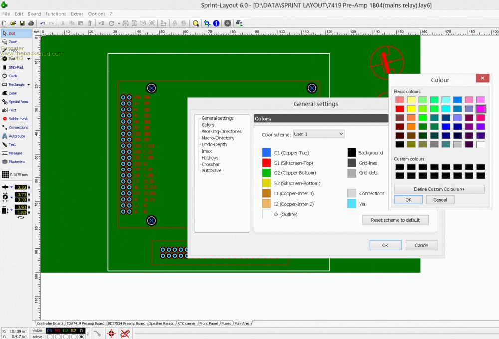
Generally speaking, you need to know the board size before you lay any tracks, but seeing as you are doing it the other way around..... 
The easiest way FOR ME that I have found, is to set the board dimensions larger then the board you are planning to design, then adjust the OUTLINE layer to suit. The PCB house will use the outline layer, to set the actual size of the board, regardless of the size you set in NEW BOARD.
Example:

Note that the board size is 160 x 100, but the outline is set to 93 x 91 - the white outline box. If you sent this to the PCB house, they would make the 93 x 91 bit, and ignore the rest outside that white box - the PCB would comply with the 100 x 100 spec for $12 at SH2U, in other words, despite the board size being 160 x 100 if you see what I mean.
You can then adjust this outline in both the X and Y dimensions to enlarge or shrink your board size to suit whatever you are laying out. 
EDIT: I prefer to set the outline layer colour to magenta rather then white. Again, this is just me. The reason is that this then allows me to easily see an outline image for the board that I draw on the silkscreen, and then the magenta actual outline layer outside that, so that when they make the board, you can then have a nice neat white outline on the silkscreen layer which finishes off the board nicely.
You change that colour if you want, in OPTIONS/GENERAL SETTINGS/COLORS.
Edited by Grogster 2016-04-04
Smoke makes things work. When the smoke gets out, it stops! |
| |
Herry
Senior Member
Joined: 31/05/2014
Location: AustraliaPosts: 261 |
| Posted: 09:32pm 02 Apr 2016 |
Copy link to clipboard |
Print this post |
|
Thanks. Since posting that, I have found that the following seems to work.
Adjust the working space marker lines just as if they were tracks.
Move everything to the top left of the board (not the bottom left where the origin is marked)
Adjust board size to leave reasonable margins.
The trick is in realising that the board origin in fact the top left and not where 'origin' is indicated!
Bu as a raw newbie, I may of course be wrong!
Senior?! ĀWhatever it says, I'm a complete and utter beginner... |
| |
Grogster
Admin Group
Joined: 31/12/2012
Location: New ZealandPosts: 9985 |
| Posted: 09:35pm 02 Apr 2016 |
Copy link to clipboard |
Print this post |
|
I always set the origin to top-left.
Right-click anywhere on board there is no track or other part, select SET ORIGIN, and select top-left.
Again, that is just me......
Smoke makes things work. When the smoke gets out, it stops! |
| |
| |
Page 2 of 2 |
