
|
|
Forum Index : Microcontroller and PC projects : Rear IO Connector of CMM2
| Author | Message | ||||
bigmik Guru Joined: 20/06/2011 Location: AustraliaPosts: 2870 |
GDay Geoff, Team, All, I have a query about the pin numbering of the rear IO header. From the CMM2 Manual page it it shows the numbering as below: 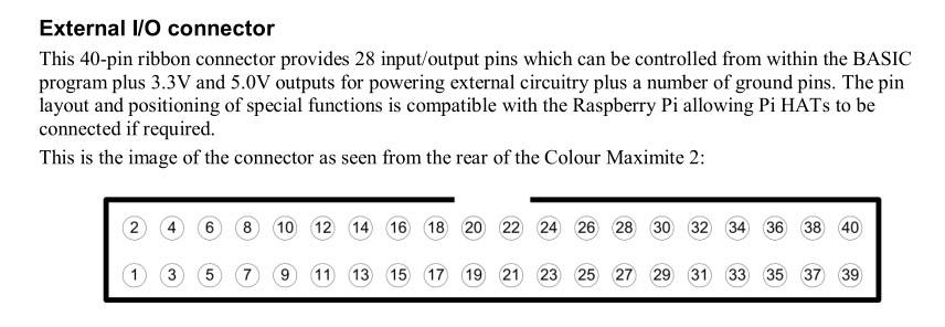 Note! Pin 1 is bottom left and the notch for the key is on the top just above pins 20 and 22. The schematic shows pin 1 of the header goes to CMM2 pin 1 on IO header 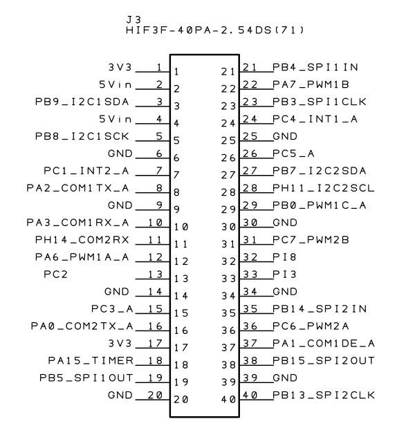 However the datasheet for the right angle header shows that the notch is correcly located on the top of the header but pin 1 is really the TOP RIGHT as shown below. 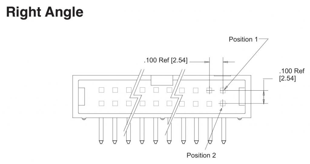 Is there an error here? Should the drawing on page 8 of the CMM2 manual have the notch on the bottom? I am not sure that such a part exists but it may do, which explains things if it does. Kind Regards Mick Mick's uMite Stuff can be found >>> HERE (Kindly hosted by Dontronics) <<< |
||||
TassyJim Guru Joined: 07/08/2011 Location: AustraliaPosts: 5898 |
The CMM2 manual description is correct. The notch is at the top and pin 1 lower left. Somewhere in the manual it describes the 'reset' feature where you short pins 39 and 40 during power-up. They are described as being the pins closest to the USB connectors. That confirms the pin arrangement. I agree that the datasheet for the connector has the alternative pin assignment but in this case, stick with the manual. The pins are arranged to match RPi pinouts so the readily available breakout boards work. In my case I had to reverse one of the 40way connectors on the supplied cable so things went together the right way. RPis don't have to worry because they have bare pins without any surround and it is up to the user to get it right. I have some short IDE extension cables which I use so I am not continually plugging into the main connector. Cheaper to replace a cable! Jim VK7JH MMedit MMBasic Help |
||||
| bigmik Guru Joined: 20/06/2011 Location: AustraliaPosts: 2870 |
Hi Jim, All, Not a problem, I have designed a breakout board to go with the CMM2 and I wanted to make sure my header was oriented correctly. 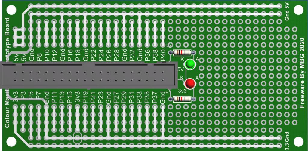 Kind Regards Mick EDIT** BTW, All those fat white lines are on the silk screen to show connectivity when fitting parts.. They reflect the traces that are (mostly) on the underside of the board. Kind Regards Mick Edited 2020-05-25 15:50 by bigmik Mick's uMite Stuff can be found >>> HERE (Kindly hosted by Dontronics) <<< |
||||
| Andrew_G Guru Joined: 18/10/2016 Location: AustraliaPosts: 840 |
Hi Mick, When the dust settles I'll put my hand up for some of these. Cheers, Andrew |
||||
| bigmik Guru Joined: 20/06/2011 Location: AustraliaPosts: 2870 |
Hi Andrew, All, I will certainly be ordering some in, when the design is finalised, but I will also be putting the Gerbers online for anyone to make them if they feel so inclined. I also have a little idea that plugs into those socket type bread boards. 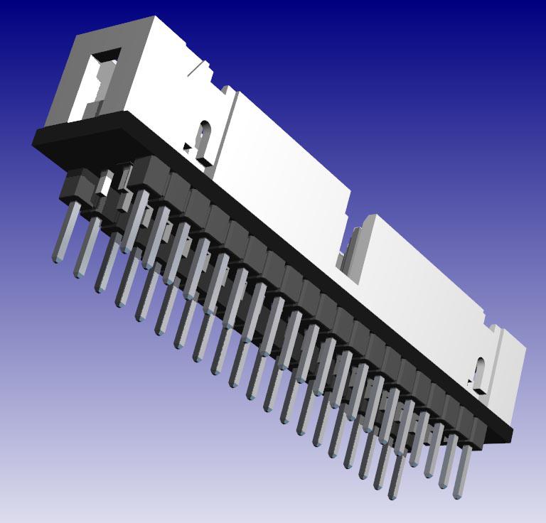 Which reminds me I have to flip the 3D image on that as it is now the wrong way around.. �  Kind Regards Mick EDIT*** OMG... Look at the size of that image.. How can I control the visual size? Mik Edited 2020-05-25 16:26 by bigmik Mick's uMite Stuff can be found >>> HERE (Kindly hosted by Dontronics) <<< |
||||
| TassyJim Guru Joined: 07/08/2011 Location: AustraliaPosts: 5898 |
Size isn't everything Mick. But I do like the idea. I get annoyed when my RPi breakout takes up too many holes on my breadboard. It would also be handy for veroboard users. Jim VK7JH MMedit MMBasic Help |
||||
| Andrew_G Guru Joined: 18/10/2016 Location: AustraliaPosts: 840 |
Hi all, I'm not sure if this is the right thread but it seems to me that "The Team" have been remarkably clever in that an HC-12 should plug straight into CMM2's pins 4,6,8 &10 (eg using one of Mik's devices), or have I got my Tx and RX swapped? (I don't yet have one to try it out) Cheers, Andrew |
||||
| Geoffg Guru Joined: 06/06/2011 Location: AustraliaPosts: 3165 |
When I was drawing the I/O connector for the manual I used arbitrary pin numbering to make it easier for someone looking at the back of the CMM2 to relate to the table below. I was not trying to reflect the standard connector pin numbering. I think a short note in the manual will be in order. Geoff Geoff Graham - http://geoffg.net |
||||
| bigmik Guru Joined: 20/06/2011 Location: AustraliaPosts: 2870 |
Hi All, @Geoff, Not a problem, I was just concerned that the schematic had MM Pin1 going to header Pin 1 and that didn't look correct. Strictly speaking MM Pin 1 should be shown going to Header pin 40 and so on flowed through.. It could be an issue if trying to buzz something out from the schematic. It stems from a VERTICAL DiL header can go either way around but a R/A one can only go Right to Left in pin numbers. All that aside, it makes sense to have IO numbering going from Left to Right so from that perspective it is designed as it should be.. I was just concerned as I was designing some development boards and of course I needed to make sure the polarity was correct. All good! Once I know the pin numbers are not the 'conventional header pin numbers' all is good. Kind Regards Mick Mick's uMite Stuff can be found >>> HERE (Kindly hosted by Dontronics) <<< |
||||
| matherp Guru Joined: 11/12/2012 Location: United KingdomPosts: 8578 |
The pin numbering on the CMM2 is exactly the same as the Raspberry Pi and deliberately so. https://www.raspberrypi-spy.co.uk/2012/06/simple-guide-to-the-rpi-gpio-header-and-pins/ |
||||
| panky Guru Joined: 02/10/2012 Location: AustraliaPosts: 1094 |
Without wishing to start a "semantics war" , if you look at the Rasberry Pi connector from above the board as it is shown in all the diagrams, pin 1 is lower left of the vertical male connector.If you now replace the vertical connector with a right angle one "and rotate the board so that you are looking directly at the pins", pin 1 now is the upper right! Happy days  , everyone is correct! The schematic is correct, the pinout agrees with RPi and the vendors pinout of their right angle connector (when viewed looking directly into the pins) is correct! , everyone is correct! The schematic is correct, the pinout agrees with RPi and the vendors pinout of their right angle connector (when viewed looking directly into the pins) is correct!... almost all of the Maximites, the MicromMites, the MM Extremes, the ArmMites, the PicoMite and loving it! |
||||
| GregZone Senior Member Joined: 22/05/2020 Location: New ZealandPosts: 114 |
Just thought I'd mention that I also found the first diagram in the OP to have the keyway on the opposite side to what I would have expected. ie. It shows the keyway as being on the even number connector side. Whereas in my experience, I believe the normal convention is for the keyway to be on the odd numbered side of the connector (as is shown in the "Right Angle" image). The comparison to the RPi connectior pin numbering doesn't show this of course, as the RPi connector is simply a double row male header (without the plastic shell that would contain the keyway cut-out). Hopefully that makes sense? Or is it just simply that for CMM2 the connector is placing the keyway on the even numbered side? (Which means a standard keyed 40 way IDE cable would have the red striped wire connected to pin 40, instead of the usual pin 1 indication) Apologies, if I've got myself completely confused over the above discussion thread. |
||||
| matherp Guru Joined: 11/12/2012 Location: United KingdomPosts: 8578 |
The only shrouded right angle headers I was able to find have the slot in the top. For layout reasons pin 1 needed to be bottom left looking at the header from the back. Substitute a non-shrouded header like Wurth Elektronik, WR-PHD, 40 Way, 2 Row, Right Angle Pin Header RS Stock No. 828-1749 Mfr. Part No. 61304021021 And the problem goes away but the shrouded one is much cheaper �0.52 vs �1.18 |
||||
| GregZone Senior Member Joined: 22/05/2020 Location: New ZealandPosts: 114 |
Thanks @matherp for that clarification. I now completely understand. I've had similar connector orientation challenges with PCB routing. :) A non-shrouded header would seem to avoid the issue. Perhaps also a small note in the documentation to clarify the cable orientation if using a pre-made 40-way IDC cable. Something like: If a shrouded header is used, where the keyway is on the side with the even numbered pins (eg. at the top for a right angled header), then be aware that a standard pre-made IDC cable will likely have the red-striped side of the ribbon cable indicating pin 40, instead of the expected pin 1. Just a thought. |
||||
Cyber Senior Member Joined: 13/01/2019 Location: UkrainePosts: 161 |
Hello. Please share what software did you use to render this image? |
||||
| bigmik Guru Joined: 20/06/2011 Location: AustraliaPosts: 2870 |
Hi Cyber, I am in the finalising stage of this board.. I use DEXPCB (from DEXPCB.COM) to design my boards. The 3D is part of the package. Once i am happy that all is Ok I will be releasing the DEX files as well as gerbers so anyone can produce them if they wish.. I will be offering them, In my usual Commercial thread on TBS, as part of my >>> PCB Repertoire <<< Kind Regards Mick Mick's uMite Stuff can be found >>> HERE (Kindly hosted by Dontronics) <<< |
||||
| Cyber Senior Member Joined: 13/01/2019 Location: UkrainePosts: 161 |
Thanx, Mick! I was surprised you could design layout of components on prototyping board in this soft. Is there ready templates for prototyping boards? So you can measure how components fit in. As well as solder maid traces. Or did you just designed prototyping board from scratch? |
||||
| bigmik Guru Joined: 20/06/2011 Location: AustraliaPosts: 2870 |
Hi Cyber, There is a `matrix' layout command but I have never used it.. I set the grid to the pad spacing (I actually used Vias but Pads are fine as well). Placed one column of 6 pads manually (Easy as) then copied that row and pasted to the next grid then copied both and pasted two rows then copied 4 rows and pasted etc etc took about 2 minutes to lay the grid out then I deleted (for where I decided to add mounting holes for example) or added another pad as needed. The array of pads was not difficult nor time consuming.. Kind Regards Mick PS. I have just sent them off to be made. Mik Mick's uMite Stuff can be found >>> HERE (Kindly hosted by Dontronics) <<< |
||||
| Cyber Senior Member Joined: 13/01/2019 Location: UkrainePosts: 161 |
So straightforward simple yet very effective! I tend to stick to such ways of doing thing. I actually often use protoboards to build my final devices (not prototypes). It is my fun hobby projects so I'm totally ok with it. And it saves me time and hassle of designing and producing PCBs. Yet I spend much time designing layout of components and traces, because I tend to fit components onto as small protoboard as possible. And I kinda like this process. In fact I face myself with many restrictions, but it's fun. I design my layouts on checkered sheets, redrawing it over and over, until I'm happy with the result. Now I wish to try the technique Mick described. Thanx again, Mick! |
||||
