
|
|
Forum Index : Microcontroller and PC projects : ST7789 SPI display without CS?
| Page 1 of 2 |
|||||
| Author | Message | ||||
| Mixtel90 Guru Joined: 05/10/2019 Location: United KingdomPosts: 8778 |
Is this supported now or is it still necessary to modify the board? I made the mistake of getting one without knowing enough to sort this out first. I might even have to connect it to an Arduino! :( Mick Zilog Inside! nascom.info for Nascom & Gemini Preliminary MMBasic docs & my PCB designs |
||||
| matherp Guru Joined: 11/12/2012 Location: United KingdomPosts: 11239 |
It should work stand-alone but will not co-exist with an SDcard. Note on the PicoMite the ST7789 has not been tested but the code was lifted from the ArmmiteL4 where it did work |
||||
| Mixtel90 Guru Joined: 05/10/2019 Location: United KingdomPosts: 8778 |
Ah... right. It's not working on this PicoMite at the moment anyway. I've used the same SPI settings that I used for the ILI9341, with the ST7789 settings obviously. No panic, I have other things to do. lol Mick Zilog Inside! nascom.info for Nascom & Gemini Preliminary MMBasic docs & my PCB designs |
||||
| Plasmamac Guru Joined: 31/01/2019 Location: GermanyPosts: 611 |
Hi , Display with cs Maybe this is usefull to create a better support. Thx Edited 2021-07-01 23:55 by Plasmamac Plasma |
||||
| Mixtel90 Guru Joined: 05/10/2019 Location: United KingdomPosts: 8778 |
Thanks, Plasma, but I was trying to avoid that for various reasons, failing eyesight and less manual dexterity than I used to have being only two of them. :) It might get paired up with an arduino for something as there's a library for it. Mick Zilog Inside! nascom.info for Nascom & Gemini Preliminary MMBasic docs & my PCB designs |
||||
bigmik Guru Joined: 20/06/2011 Location: AustraliaPosts: 2980 |
Hi Mick (From Mick), You should be able to create a work around by ANDing the SCL with your own CS signal and feeding it to the SCL of your display.. If you need a cct let me know and I will try to remove the clouds from my brain. Regards, Mick (the other Mick0 Mick's uMite Stuff can be found >>> HERE (Kindly hosted by Dontronics) <<< |
||||
| bigmik Guru Joined: 20/06/2011 Location: AustraliaPosts: 2980 |
Hi Mick, All, I had a little think about this, I think this might work for you (haven't tested it) Use a couple of schottky diodes and a pull down resistor. You may have to fiddle with the pull down value a bit but it logically looks ok to my feeble brain. You wont get an SCL signal to your display unless BOTH the SCL is low and the CS is low 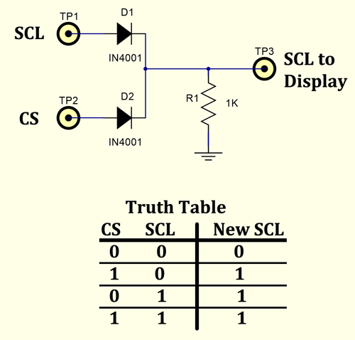 Regards, The other Mick Mick's uMite Stuff can be found >>> HERE (Kindly hosted by Dontronics) <<< |
||||
| matherp Guru Joined: 11/12/2012 Location: United KingdomPosts: 11239 |
The normal discrete and gate has a pullup on the output and the diodes the opposite way round. 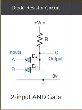 |
||||
| phil99 Guru Joined: 11/02/2018 Location: AustraliaPosts: 3163 |
Which circuit to use depends on whether a 1 is high or low. I think active low is required here so BigMick's version is the one to use. |
||||
| bigmik Guru Joined: 20/06/2011 Location: AustraliaPosts: 2980 |
Peter, Phil, All, What I was saying is what is we we used to call negative logic as I was brought up with computers in the 70's and 80' most (as is today to some extent) signals we dealt with were NEGATIVE active ie. LOW is active signal. SPI is High in idle mode so I worked on ANDING. The LOW with a LOW CS to give a LOW to the TFT. You are correct in that an AND gate in its purist form is H AND H = H The translation is change the shape and change all of the bubbles So `MY' interpretation of AND is an AND symbol with bubbles on the inputs and a bubble on the output (This is negative logic) It will equate to an OR gate in the traditional manner that you see in data sheets and manuals. The way it was explained to me was it made fault finding easier as you could see what was expected (if the input or output had a bubble is was LOW active, if no bubble it would be HIGH active) I can see how I may have mislead you and others but I feel my circuit suggestion is correct, just my terminology `may' be dated as I learned it so long ago and I have not been to formal electronics education in 30+ years. Peter, your diagram is indeed an AND gate in traditional logic, but that idea will not work to help Mick with his problem. Later I will upload some diagrams to explain what I mean, it is just a force of habit going back longer than time itself (Except for Paul_L, he says he is older than time) But honestly, if I did say an OR gate it is harder to explain how the circuit works. Kind Regards, Mick Mick's uMite Stuff can be found >>> HERE (Kindly hosted by Dontronics) <<< |
||||
| Paul_L Guru Joined: 03/03/2016 Location: United StatesPosts: 769 |
Care to try to explain the difference between AND and NOR????  Paul in NY Edited 2021-07-03 11:50 by Paul_L |
||||
| bigmik Guru Joined: 20/06/2011 Location: AustraliaPosts: 2980 |
Hi All, As Promised earlier. Here is a snippet from >>> This PDF <<< on Negative Vs Positive logic (Page 3 of 8) 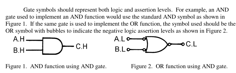 This is showing the Reverse of mine as an AND in positive logic and how it should look in as an OR in negative logic. Note the shape changes and the inputs/outputs all toggle the bubbles. @Paul_L Do you really want an answer to totally confuse every one? A NOR is simply an OR followed by a NOT (Inverter) on the output. Then of course there is XOR or exclusive OR.. (Crikey where is this coming from, I learned all that 122 years ago. I thought I forgot it all.  Regards, Mick Edited 2021-07-03 14:44 by bigmik Mick's uMite Stuff can be found >>> HERE (Kindly hosted by Dontronics) <<< |
||||
| phil99 Guru Joined: 11/02/2018 Location: AustraliaPosts: 3163 |
AND IN 1 IN 2 OUT " 0 0 0 " 0 1 0 " 1 0 0 " 1 1 1 OR IN 1 IN 2 OUT " 0 0 0 " 0 1 1 " 1 0 1 " 1 1 1 NOR IN 1 IN 2 OUT " 0 0 1 " 0 1 0 " 1 0 0 " 1 1 0 |
||||
| Mixtel90 Guru Joined: 05/10/2019 Location: United KingdomPosts: 8778 |
And just for completeness: NAND IN 1 IN 2 OUT " 0 0 1 " 0 1 1 " 1 0 1 " 1 1 0 XOR IN 1 IN 2 OUT " 0 0 0 " 0 1 1 " 1 0 1 " 1 1 0 The number of times I've scribbled truth tables on bits of paper over the years while I've been working something out! LOL They aren't something I tend to use every day... I'll have a go at gating CS and SCL. It's probably on the back burner for a few days while I have my programming head on though. Mick Zilog Inside! nascom.info for Nascom & Gemini Preliminary MMBasic docs & my PCB designs |
||||
| bigmik Guru Joined: 20/06/2011 Location: AustraliaPosts: 2980 |
Hi Mick, All, My idea was to simplify things. I don't know for sure if it will work 100% with the 2 x diodes and 1 x pull down. Too high a pull down wont get the drive for the TFT too low will draw current when the TFT is not accessed. An AND gate (Negative logic, OR gate in Conventional/Positive logic) would probably be the preference but requires extra `bodging' to get it to work. Let me know how you go with it. Regards, Mick Mick's uMite Stuff can be found >>> HERE (Kindly hosted by Dontronics) <<< |
||||
| Mixtel90 Guru Joined: 05/10/2019 Location: United KingdomPosts: 8778 |
It looks fair enough, Mick. I'd try it now but I took the display off the board and put it away - and it's the same Pico that I'm using for the PIO assembler so the less flakey bits on there the better really. :) Schottky diodes would be good to get a better defined low. Pull-up resistor shouldn't be too bad, but too high and it slows the gate down. Many, many, many moons ago we used to use some logic boxes that were designed by the school. BILLIE - Binary Input Logic Link Instructional Equipment. They were basically 4-stage dividers with 4 lights on the top and 4mm plugs & sockets to change their configuration in various ways. A multi-pin plug & socket allowed them to be stacked end to end along a bench. All in nice polished wood cases. I wouldn't have mentioned them but they used RTL, which you obviously have a liking for. :) Mick Zilog Inside! nascom.info for Nascom & Gemini Preliminary MMBasic docs & my PCB designs |
||||
| Mixtel90 Guru Joined: 05/10/2019 Location: United KingdomPosts: 8778 |
I tried your circuit, Mick. Partial success. At least the screen lights, but gui test, text and cls(colour) do nothing. 10k was too high to work, 1k gave these results. I went for 1n4148 diodes as they were handy - and are probably more suited to this job anyway. Not sure what they did on the module, but on the chip CS is active low and data seems to be read on the rising edge of SCL. It might be a timing issue, I suppose. Edited 2021-07-04 05:21 by Mixtel90 Mick Zilog Inside! nascom.info for Nascom & Gemini Preliminary MMBasic docs & my PCB designs |
||||
disco4now Guru Joined: 18/12/2014 Location: AustraliaPosts: 1109 |
Extract from post linked below. I have a couple of these ST7789 clones that come without the CS pin exposed. I have the source for Peter's driver for the MM2 and MM+ but have not been able to get it to go as is i.e. with CS permanently selected on the board. Apparently when they work with Arduino, they use SPI mode 3 but I have no success. In the end I modified it to expose the CS pin in lieu of the BLK pin that is not really required. It works with Peter's drivers for MM2 and MM+ and natively supported on the ARMMites. I have not tested on Picomite yet but here is link to original post where I modified it to work with Armmite L4 Adding CS pin F4 H7FotSF4xGT |
||||
| bigmik Guru Joined: 20/06/2011 Location: AustraliaPosts: 2980 |
Hi MICK, All, If it was me I would do the modification as Disco4now suggested, it looks fairly easy. Can you provide more detail on this model display as I wouldn't mind experimenting with one? Re my circuit, sorry it didn't work as expected, I was worried about timing hence why I selected Schottky diodes.. plus they should give a higher HI as they only drop .2-.3v compared to your IN914 of .6-.7v which would drop the high to say 2.6v you should get about 3v using schottky. It is a tricky one, I wonder why they didnt bring the CS out to at least solder jumper option pads. You could try dropping the resistor to 470R or even trying a 100nf in parallel to the resistor to slightly extend/delay the SCL to the display.. it may or may not work.. A gate might be a much better option, besides the mod, look for a chip that can run off 3v3 and is reasonably fast.. Regards, MICK Mick's uMite Stuff can be found >>> HERE (Kindly hosted by Dontronics) <<< |
||||
| Mixtel90 Guru Joined: 05/10/2019 Location: United KingdomPosts: 8778 |
I'm doubtful if I could do the mod to the display now, Mick. My efforts with fine soldering haven't been very successful recently. It would have been *nice* to put it on the PicoMite, but it's by no means essential and these displays aren't expensive. This is the display I ordered. Having finally had a proper look at the back it's not quite the same: https://www.ebay.co.uk/itm/393093456134?ssPageName=STRK%3AMEBIDX%3AIT&_trksid=p2060353.m2749.l2649 Although connections are the same, the pcb on the one I received isn't laid out the same as either the one used for the mod or the picture on ebay! All the ebay pics for the 1.3" model seem to show the same version, but goodness knows what you'll actually get if you order one. 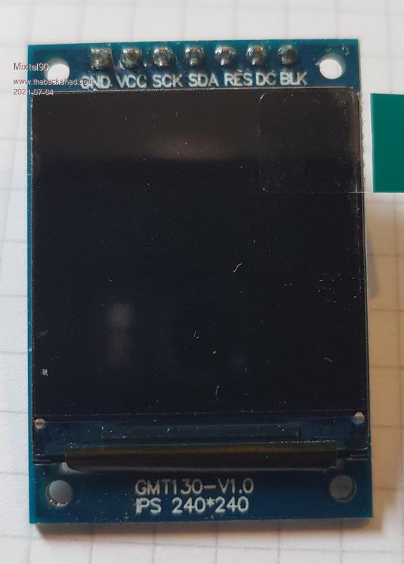 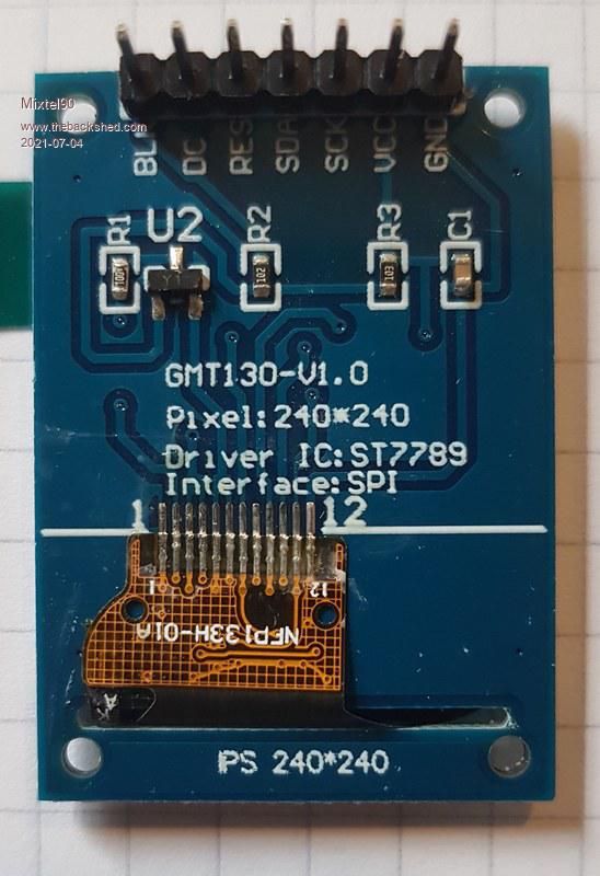 Edited 2021-07-04 22:47 by Mixtel90 Mick Zilog Inside! nascom.info for Nascom & Gemini Preliminary MMBasic docs & my PCB designs |
||||
| Page 1 of 2 |
|||||
| The Back Shed's forum code is written, and hosted, in Australia. | © JAQ Software 2026 |
