
|
|
Forum Index : Microcontroller and PC projects : Pico I2S/RTC super-HAT
| Author | Message | ||||
| matherp Guru Joined: 11/12/2012 Location: United KingdomPosts: 11314 |
Another quick design 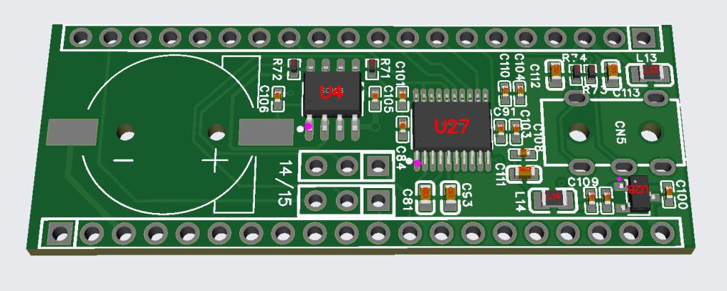 Schematic ef24a008-bf00-4508-9bfe-93c89e591622.pdf OPTION AUDIO I2S GP6,GP5 OPTION SYSTEM I2C GP14, GP15 (or GP26,GP27) I'll get some made to test the I2S bit as this is a new module. Assuming all OK I'll post the gerbers etc. Plug a Pico2 into this and this into a Waveshare display and you have everything needed for a high quality music player |
||||
| matherp Guru Joined: 11/12/2012 Location: United KingdomPosts: 11314 |
The boards have arrived and work perfectly. I2S audio and DS3231 RTC on a simple Pico "Hat". Since getting these built I've also added a miniature reset switch but you can omit that on the BOM if not required. NB: the BOM includes simple 20-way headers. I omitted these and used long-pin variants so the boards can be stacked. I can't find a part number for these on JLC/LCSC. As always, omit any parts you prefer to solder yourselves to save cost - Audio jack/battery holder, jumpers etc. The underside of the board specifies the option commands need to configure. The PCM5102A I2S DAC runs off its own linear regulator with extensive decoupling/filtering and audio quality is superb. The boards could be hand soldered but use numerous 0402 parts so pretty tricky. OPTION SYSTEM I2C GP14,GP15 or OPTION SYSTEM I2C GP26,GP25 OPTION AUDIO I2S GP6,GP5 NB: I will be enabling I2S audio on all Pico variants (RP2040 and RP2350) in a future release as it is SO GOOD  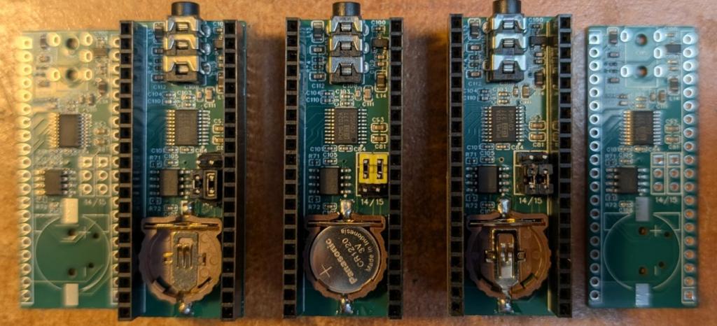 Schematic 1c207f3e-630a-4dcf-b3ca-276b52e8f31e.pdf 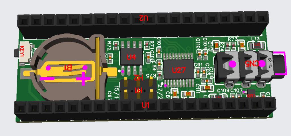 Design file PicoI2SRTC.zip Gerbers Gerber_PCB1_2025-02-04.zip BOM and P&P BOM_Board1_PCB1_2025-02-04.zip Edited 2025-02-04 23:16 by matherp |
||||
| Volhout Guru Joined: 05/03/2018 Location: NetherlandsPosts: 5873 |
Hi Peter, In 2040 VGA this I2S occupies both PIO's correct ? Volhout PicomiteVGA PETSCII ROBOTS |
||||
| matherp Guru Joined: 11/12/2012 Location: United KingdomPosts: 11314 |
Correct, but it is a user choice to use it rather than PWM, VS1053, or SPI DAC Or can it be a separate application on the VGA PIO? What are the limitations other than number of program slots? Edited 2025-02-04 23:36 by matherp |
||||
| Volhout Guru Joined: 05/03/2018 Location: NetherlandsPosts: 5873 |
Peter, I have no idea what the VGA PIO code is. Never seen it. Is it this ? 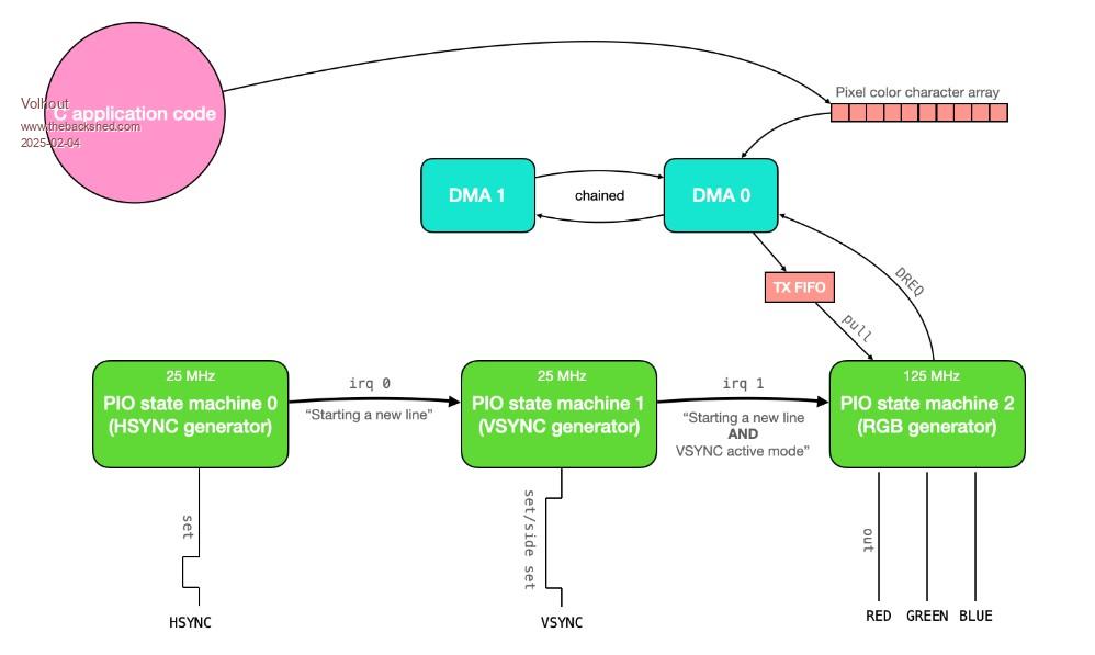 If I counted right, 31 of the 32 instructions are used. When there is a state machine in that pio free (seems so), and there are program memory locations (there are ony 32 total, 31 used) available then both may be combined. How large is the I2S code ? Does it use only 1 state machine ? I looks hopeless, but what is the size of your I2S code.? Volhout Edited 2025-02-04 23:58 by Volhout PicomiteVGA PETSCII ROBOTS |
||||
| matherp Guru Joined: 11/12/2012 Location: United KingdomPosts: 11314 |
VGA is 16 instructions and uses a couple of DMA channels I2S is 7 instructions, doesn't use DMA, but uses a combined TX FIFO ; ============================================================================ ; QVGA PIO (16 instructions) ; ============================================================================ ; Control word (right shifted): ; - bit 0..26 (27 bits) loop counter N ; - bit 27..31 (5 bits) jump address .program qvga .side_set 2 ; HSYNC and VSYNC output (2 bits) .define NOSYNC 0 ; no sync, output image or blanking .define HSYNC 1 ; HSYNC pulse (or CSYNC pulse) .define VSYNC 2 ; VSYNC pulse .define VHSYNC 3 ; HSYNC and VSYNC pulse .define BPP 4 ; number of bits per pixel ; ===== [3 instructions] HSYNC pulse, N=delay in clock cycles - 3 ; starts HSYNC at time 0 public hsync: jmp x--,hsync side HSYNC ; [N+1] loop public entry: ; program entry point out x,27 side HSYNC ; [1] get next loop counter N out pc,5 side HSYNC ; [1] jump to next function ; ===== [3 instructions] VSYNC pulse, N=delay in clock cycles - 3 ; starts VSYNC at time 0 public vsync: jmp x--,vsync side VSYNC ; [N+1] loop out x,27 side VSYNC ; [1] get next loop counter N out pc,5 side VSYNC ; [1] jump to next function ; ===== [3 instructions] VSYNC and HSYNC pulse, N=delay in clock cycles - 3 ; starts HSYNC and VSYNC at time 0 public vhsync: jmp x--,vhsync side VHSYNC ; [N+1] loop out x,27 side VHSYNC ; [1] get next loop counter N out pc,5 side VHSYNC ; [1] jump to next function ; ===== [4 instructions] DARK pulse, N=delay in clock cycles - 4 ; sets blanking at time 0, starts NOSYNC at time 0 public dark: mov pins,null side NOSYNC ; [1] dark output dark_loop: jmp x--,dark_loop side NOSYNC ; [N+1] loop .wrap_target ; wrap jump target out x,27 side NOSYNC ; [1] get next loop counter N out pc,5 side NOSYNC ; [1] jump to next function ; ===== [3 instructions] output pixels at 5 clocks per pixel, N=number of pixels-2 ; number of pixels must be multiple of: 1 at BP=32, 2 at BPP=16, 4 at BPP=8, 8 at BPP=4, 16 at BPP=2, 32 at BPP=1 ; Output first pixel at time 0 public output: out pins,BPP side NOSYNC [2] ; [3] output pixel jmp x--,output side NOSYNC [1] ; [2] loop (N+1 pixels) out pins,BPP side NOSYNC [2] ; [3] output pixel .wrap ; wrap jump to .wrap_target 0xe03e, // 0: set x, 30 side 0 0x8880, // 1: pull noblock side 1 0x6001, // 2: out pins, 1 side 0 0x0842, // 3: jmp x--, 2 side 1 0xf03e, // 4: set x, 30 side 2 0x9880, // 5: pull noblock side 3 0x7001, // 6: out pins, 1 side 2 0x1846, // 7: jmp x--, 6 side 3 PIO assemble 1 .program i2s .side set 2 .wrap target .line 20 Set x,30 side 0 Pull noblock side 1 .label loop1 Out pins,1 side 0 Jmp x--,loop1 side 1 Set x,30 side 2 Pull noblock side 3 .label loop2 Out pins,1 side 2 Jmp x--,loop2 side 3 .wrap .end program list Edited 2025-02-05 01:21 by matherp |
||||
| Volhout Guru Joined: 05/03/2018 Location: NetherlandsPosts: 5873 |
Hi Peter, Saw your PM, and will do a bit of reading, although I have an idea how they use it from looking at the code, and knowing how video is made. I am not certain how the C environment assembler works, but what I would do is: 1/ I think the code is fast enough, and there is plenty of room. I would re-write the code to avoid .wrap and .wrap target (replace .wrap with a JMP 16 (or JMP 20). That makes it independent of the assembler of the VGA code that uses WRAP for timing accuracy. 2/ simply paste the I2S mnemonics right after the VGA code. Do not configure anything yet. Assemble the stuff (compile a VGA project) and see if it runs. If it runs, the current implementation does not use any of the PIO memory or PIO0 after location 16. You can of coarse also use location 20... If it does not run, stop the project. PIO is operating outside it's program area (maybe for timing, since locations 16..31 are default filled with 00 which is JMP 0). 3/ assuming all is well, This could then be part of your generic setup, in all VGA product. All VGA binaries would have I2S build in. Only when OPTION I2S is found it will assign GPIO pins (configure the state machine) and start the state machine. Volhout Oops..you cannot change .wrap in JMP since it violates the BCLK.. -> plan B Edited 2025-02-05 04:07 by Volhout PicomiteVGA PETSCII ROBOTS |
||||
| Volhout Guru Joined: 05/03/2018 Location: NetherlandsPosts: 5873 |
Peter, It is actually quite smart what they do. Easy to change resolution, timing, etc.. But it requires the ARM to support VGA heavily. The VGA data is coming from the DMA, but every line requires 2x support from the ARM: number of pixels, and timing of HSYNC. the use of OUT PC,5 gives the possibility to jump everywhere in the program. An they use the dark_loop: for all timing loops. I also got what you are trying to do. Assemble the VGA and I2C in the MMBasic assembler, and write the binary blob into PIO memory. Smart... Good luck, I hope it works. Volhout P.S. the OUT PC,5 does not assemble correct..? I have used PC also in the quadrature decoder, but as an offset in a JMP. Apparently that worked. PicomiteVGA PETSCII ROBOTS |
||||
| The Back Shed's forum code is written, and hosted, in Australia. | © JAQ Software 2026 |
