
|
|
Forum Index : Microcontroller and PC projects : Proof of concept - PGA2350-CPM (ColourPicoMite)
| Author | Message | ||||
| Mixtel90 Guru Joined: 05/10/2019 Location: United KingdomPosts: 8909 |
This is something that has been in development for quite a while now, ever since the PGA2350 appeared, in fact. I've kept coming back to it occasionally as it's something of a challenge. :) It's rather like a CMM 1.8. Since changing the USB-C converter for one with 3V3 signals you can even fit an on-off switch if you like. :) There are 20 GPIO pins on the rear panel and a single spare pin inside (there's not enough space for a longer connector, even though it's not a box type). The layout has been hacked about a lot since it started and is now completely re-done since it started out as my Beta design. I've now included the audio modules that I've just done for the build your own design. I think they'll work but I've not checked all the signals yet. There's still a lot of work to be done and the testing so far is only very superficial. It may be of interest to those who have a PGA2350 stuck in a drawer. 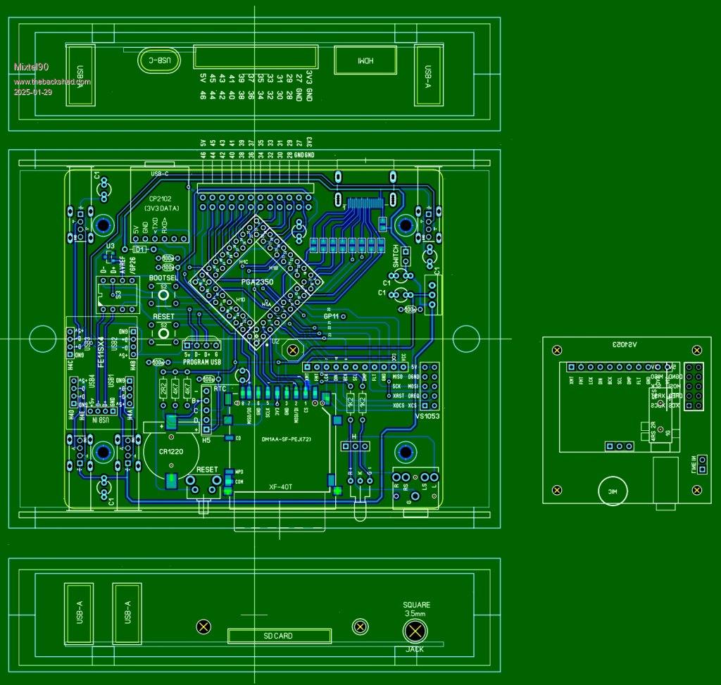 Mick Zilog Inside! nascom.info for Nascom & Gemini Preliminary MMBasic docs & my PCB designs |
||||
| Mixtel90 Guru Joined: 05/10/2019 Location: United KingdomPosts: 8909 |
Does anyone think it would be an idea to use GP0 for the PSRAM (although it needs a link under the PGA2350) to make all 8 ADC pins available on the GPIO header? It makes it a bit more fiddly to assemble so I'm not sure. I'd use GP11 on the SD card instead. Mick Zilog Inside! nascom.info for Nascom & Gemini Preliminary MMBasic docs & my PCB designs |
||||
| PhenixRising Guru Joined: 07/11/2023 Location: United KingdomPosts: 1957 |
Love it, Mick  ('cept for the lasts-five-minutes-CR1220) ('cept for the lasts-five-minutes-CR1220) |
||||
| Mixtel90 Guru Joined: 05/10/2019 Location: United KingdomPosts: 8909 |
Tough. You can always swap the whole RTC or put a remote battery holder on flying leads. I don't think I can get anything bigger in there without cutting it in half, and that's cheating. :) I'll try though... Mick Zilog Inside! nascom.info for Nascom & Gemini Preliminary MMBasic docs & my PCB designs |
||||
| PhenixRising Guru Joined: 07/11/2023 Location: United KingdomPosts: 1957 |
Yeah I already have these for the CR123 |
||||
| Mixtel90 Guru Joined: 05/10/2019 Location: United KingdomPosts: 8909 |
I think I've managed to get a CR2032 in now. :) Mick Zilog Inside! nascom.info for Nascom & Gemini Preliminary MMBasic docs & my PCB designs |
||||
| Mixtel90 Guru Joined: 05/10/2019 Location: United KingdomPosts: 8909 |
Just added two more GPIO pins by moving the USB-C module. GP47 and another GND pin, so all GPIO pins from GP27 to GP47 are available. PSRAM CS is now on GP0 so you have to put a flying lead in for that. I've included a pad for it under the PGA2350 so it's hidden nicely. :) There is also a hole that you can use to thread the wire down through to connect it under the board if you wish. I'd considered a pogo pin but the target pad is a bit small. The VS1053 SPK socket has to be wired to the header underneath it so it can be connected to the front panel socket. That's deliberate as I only want a single design for the front panel. Audio socket moved slightly as the LINE IN header on the VS1053 was just hitting it. The DVI traces have been twiddled to get their lengths a bit more similar. Mick Zilog Inside! nascom.info for Nascom & Gemini Preliminary MMBasic docs & my PCB designs |
||||
| stanleyella Guru Joined: 25/06/2022 Location: United KingdomPosts: 2807 |
The DVI traces have been twiddled to get their lengths a bit more similar. I use a hdmi breakout board with surface mount 220R resistors and that seems the crucial bit, not the tracks leading to the breakout board. this strip board is stable display. just a point. stan  |
||||
| Mixtel90 Guru Joined: 05/10/2019 Location: United KingdomPosts: 8909 |
I have one of those but it won't fit in this case. I've specified it for the "build your own Pico" design, where you can plug in boards for LCD or VGA into the same connector. I don't think the location of the resistor along the trace is important. It's value is far to high for it to be used as a line terminator to control the cable connection. The 220R/270R is to protect the output of the GPIO pin as the other end has 75R to ground. That would sag the output voltage from the Pico badly and take it out of spec. Mick Zilog Inside! nascom.info for Nascom & Gemini Preliminary MMBasic docs & my PCB designs |
||||
| stanleyella Guru Joined: 25/06/2022 Location: United KingdomPosts: 2807 |
I sort of like the idea of vga,hdmi and glcd on one board. I could mount my vga, hdmi and glcd boards... but why. I got vga and hdmi into same monitor, only one displayed at a time. can't really see the point of stacking them unless they interacted via i2c or serial |
||||
| Mixtel90 Guru Joined: 05/10/2019 Location: United KingdomPosts: 8909 |
GP27 is now the pin that can be switched to GND (now via a safety resistor). GP26 has moved to SD card CS and the other SD pins have moved around. GP1 is now on the GPIO port where it can be used for FFIN. Apart from that most of today's work has been in sorting out the circuit diagram. The GPIO port now has 3V3, 5V, 3xGND pins, GP1 and all the pins from GP28 to GP47. PSRAM CS is on GP0 by default, but if you wish you wan swap it to GP47 under the board and cut a solder blob link to disconnect it from the GPIO port. Obviously you can also cut this link if you prefer not to modify your PGA2350. Mick Zilog Inside! nascom.info for Nascom & Gemini Preliminary MMBasic docs & my PCB designs |
||||
| Mixtel90 Guru Joined: 05/10/2019 Location: United KingdomPosts: 8909 |
More musings... Is it worth sacrificing two GPIO pins to bring out System I2C? It's easy enough to rearrange the port to give GP1, SDA, SCL, COM1_TX/GP28, COM1_RX/GP29, GP30-GP37 and GP40-GP47. Still keeping the supply and GND pins. GP30 and GP31 are also I2C2. The only real advantage to bringing it out is to connect I2C controllers that need it, I think. Mick Zilog Inside! nascom.info for Nascom & Gemini Preliminary MMBasic docs & my PCB designs |
||||
| The Back Shed's forum code is written, and hosted, in Australia. | © JAQ Software 2026 |
