
|
|
Forum Index : Microcontroller and PC projects : Picomite issues with MCP3002, dual channel ADC SPI
| Author | Message | ||||
| apalert Newbie Joined: 06/07/2023 Location: AustraliaPosts: 31 |
Have connection but data returned is rubbish. Any tips or clues gladly appreciated. My code below is modified from Appendix D in Picomite User Manual OPTION BASE 1 ' array will start with the index 1 DIM data%(2) 'array for receiving channel 1 data dim data2%(2) 'array for receiving channel 2 data SETPIN GP8, GP15, GP14, SPI2 ' assign the I/O pins, RX, TX, CLK PIN(27) = 1 : SETPIN 27, DOUT 'pin 27 ADC chip enable active low SPI2 OPEN 5000000, 1, 8 ' speed is 5MHz, 8 bits data PIN(27) = 0 ' assert the enable line (active low) SPI2 WRITE 2, 104, 0 ' initialise ADC channel 0 SPI2 READ 2, data%() ' get two bytes from ADC SPI2 WRITE 2, 120, 0 ' initialise ADC, channel 1 SPI2 READ 2, data2%() ' get two bytes from the slave PIN(27) = 1 ' deselect the slave SPI2 CLOSE ' and close the channel 'output to console ? bin$(data%(1)), bin$(data%(2)), bin$(data2%(1)), bin$(data2%(2)) |
||||
jwettroth Regular Member Joined: 02/08/2011 Location: United StatesPosts: 75 |
The part supports SPI at 3.2 at 5v and 1.2 at 3.3. Change you speed to something reasonable- 1 Mhz? John Wettroth |
||||
| apalert Newbie Joined: 06/07/2023 Location: AustraliaPosts: 31 |
Good point, tried a range of speeds all the way down to 100kHz. No joy. |
||||
| Volhout Guru Joined: 05/03/2018 Location: NetherlandsPosts: 5028 |
First things I would try - change SPI to mode 0 ( the most common mode) - wait between SPI write and SPI read, to give the adc time to perform its conversion Volhout PicomiteVGA PETSCII ROBOTS |
||||
| phil99 Guru Joined: 11/02/2018 Location: AustraliaPosts: 2582 |
Another short Pause between Enable and Write may also be needed if the chip sleeps when idle. |
||||
TassyJim Guru Joined: 07/08/2011 Location: AustraliaPosts: 6266 |
I think you need to send the channel setup data and receive the results in one command. Use 16 bits not 8 ' SPI2 OPEN 1000000, 0, 16 Ch0data = SPI2(Ch0config) Ch1data = SPI2(Ch1config) I don't have a chip to test with. Jim Edited 2025-01-31 16:48 by TassyJim VK7JH MMedit |
||||
| Volhout Guru Joined: 05/03/2018 Location: NetherlandsPosts: 5028 |
So summary: - do not use a clock higher that 1MHz (the chip does 2 MHz max at 3.3V) - use 16 bit transfers (or 2x8 bit transfers as below) - you need to mask the read ADC value, since the MSB's are determined by pullup or pulldown. - you need to use SPI mode 0 (called "0.0" in the datasheet). in essence this chip understands SPI mode 0 and 3, but not 1 and 2. - you need to receive data while sending. use the function value = SPI2( data ) Do not use commands SPI WRITE and SPI READ, since these do not operate at the same time. as TassyJim said: SPI2 OPEN 1000000,0,16 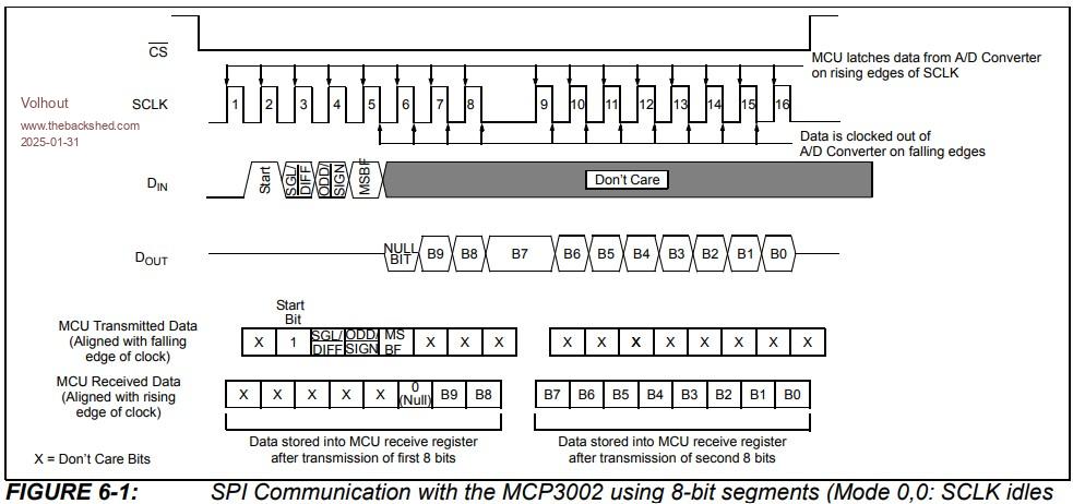 Regards, Volhout Edited 2025-01-31 18:24 by Volhout PicomiteVGA PETSCII ROBOTS |
||||
| apalert Newbie Joined: 06/07/2023 Location: AustraliaPosts: 31 |
Many thanks for all suggestions, new version of code below. Hours have been spent tweaking. New ADC chip tried, wiring triple checked. Unfortunately output is still garbage :( Below the code is a table of data returned. I put the code in a For x= 1 to 40 loop and ran it multiple times with 1/2VDD, VDD and VSS test voltage inputs. There is a curious pattern to the garbage! SETPIN 27, DOUT ' pin 27 ADC chip enable active low PIN(27) = 1 ' ADC chip disabled SETPIN 11, 20, 19, SPI2 ' assign SPI I/O pins, RX, TX, CLK pause 20 SPI2 OPEN 100000, 0, 10 ' speed 1MHz, SPI mode 0, 10 bits data PIN(27) = 0 ' ADC chip enabled data1 = spi2(104) ' get data from ADC pin(27)=1 ' ADC chip disabled SPI2 CLOSE ' close the channel 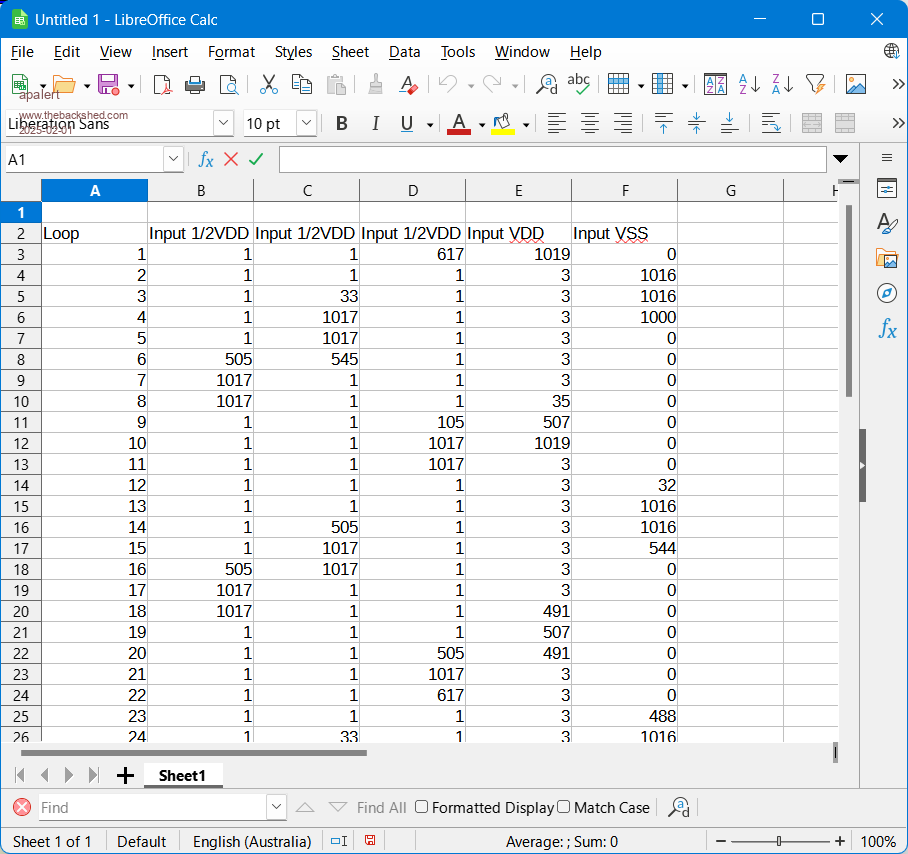 2025-02-01.png.pdf Edited 2025-02-01 17:11 by apalert |
||||
| karlelch Senior Member Joined: 30/10/2014 Location: GermanyPosts: 235 |
Hi not sure if it helps. I wrote a library for the MCP3208 (SPI, 12 bit, 8 channel), using the respective Arduino C(++) code as an example. ' lib_mcp3208.bas v0.1.2 ' ----------------------- ' MCP3208 8-channel ADC driver ' 2024-02-04 - v0.1.1 - No constants to save global variable slots ' 2024-11-25 - v0.1.2 - Test routine added ' Example: ' Const PIN_SPI2_RX = MM.Info(PinNo GP12) ' Const PIN_SPI2_TX = MM.Info(PinNo GP11) ' Const PIN_SPI2_CLK = MM.Info(PinNo GP10) ' Const PIN_MCP3208_CS = MM.Info(PinNo GP13) ' MCP3208.init PIN_SPI2_RX, PIN_SPI2_TX, PIN_SPI2_CLK, PIN_MCP3208_CS ' Dim v(3) ' MCP3208.readADCChans 4, v() ' Math V_print v() ' MCP3208.close ' --------------------------------------------------------------------------- Option Base 0 Option Explicit Option Escape Option Default Float Dim integer MCP3208.cs = MM.Info(PinNo GP13) ' =========================================================================== ' MCP3208 8-channel ADC driver ' --------------------------------------------------------------------------- Sub MCP3208.init rx%, tx%, clk%, cs% ' Setup user SPI2 Print "Initializing MCP3208 via SPI2 ..." SetPin rx%, tx%, clk%, SPI2 SetPin MCP3208.cs, DOUT Pin(MCP3208.cs) = 0 Pause 50 Pin(MCP3208.cs) = 1 SPI2 Open 1000000, 0, 8 ' 1MHz, mode 0, 8 bits Print "| Ready." End Sub Function MCP3208.readADC(ch%) ' Read channel `ch%` Local integer val, addr = &H60 Or ((ch% And &H07) << 2) Pin(MCP3208.cs) = 0 SPI2 Write 1, addr val = SPI2(0) << 4 val = val Or (SPI2(0) >> 4) Pin(MCP3208.cs) = 1 MCP3208.readADC = val End Function Sub MCP3208.readADCChans n%, dta%() ' Read channels 0 to `n%`-1 into `dta%()` Local integer i, addr For i=0 To n%-1 addr = &H60 Or ((i And &H07) << 2) Pin(MCP3208.cs) = 0 SPI2 Write 1, addr dta%(i) = SPI2(0) << 4 dta%(i) = dta%(i) Or (SPI2(0) >> 4) Pin(MCP3208.cs) = 1 Next End Sub Sub MCP3208.close ' Close SPI2 devices SPI2 Close SetPin MCP3208.cs, OFF End Sub ' --------------------------------------------------------------------------- Sub MCP3208.test Local integer rx, tx, clk, cs, i, j Local integer v(7) rx = MM.Info(PinNo GP12) tx = MM.Info(PinNo GP11) clk = MM.Info(PinNo GP10) cs = MM.Info(PinNo GP13) Print "Test is using SPI1 with:" Print " VSYS -> VDD, VREF" Print " GND -> AGND, DGND" Print " GP10 -> CLK" Print " GP11 -> DIN" Print " GP12 -> DOUT" Print " GP13 -> CS/SHDN" MCP3208.init rx, tx, clk, cs For i=0 To 50 /* For j=0 To 7 v(j) = MCP3208.readADC(j) Next */ MCP3208.readADCChans 7, v() Math V_print v() Pause 500 Next MCP3208.close End Sub It is mean to be loaded as a library, but it comes with a simple test. Here, I am varying the voltage on channel 0 (left most value) from 0V to 5V and back to 0V using a potentiometer. > mcp3208.test Test is using SPI1 with: VSYS -> VDD, VREF GND -> AGND, DGND GP10 -> CLK GP11 -> DIN GP12 -> DOUT GP13 -> CS/SHDN Initializing MCP3208 via SPI2 ... | Ready. 4, 0, 0, 0, 0, 0, 0, 0 4, 0, 0, 7, 22, 31, 69, 0 3, 60, 61, 71, 89, 107, 178, 0 90, 149, 141, 191, 242, 322, 506, 0 970, 542, 481, 532, 588, 676, 823, 0 1452, 804, 794, 832, 847, 874, 885, 0 2186, 935, 888, 858, 832, 839, 854, 0 4063, 960, 881, 807, 810, 790, 765, 0 4095, 887, 839, 764, 730, 703, 667, 0 2050, 790, 763, 693, 662, 624, 552, 0 1432, 611, 540, 431, 370, 275, 131, 0 972, 253, 202, 91, 48, 0, 0, 0 371, 25, 14, 0, 0, 0, 0, 0 4, 0, 0, 0, 0, 0, 0, 0 4, 0, 0, 8, 22, 21, 73, 0 3, 66, 59, 69, 94, 118, 190, 0 > Cheers Thomas Edited 2025-02-01 21:36 by karlelch |
||||
| karlelch Senior Member Joined: 30/10/2014 Location: GermanyPosts: 235 |
P.S.: I think in `SPI2 OPEN 100000, 0, 10` the 10 bits is the problem. The bit width refers to whether you read/write bytes (I read/write bytes) or 16 bit words to communicate with the SPI device - it is not related to the bit depth of your ADC. |
||||
| TassyJim Guru Joined: 07/08/2011 Location: AustraliaPosts: 6266 |
Including the start bit, you need 4 bits to set the configuration, one null bit and 10 data bits By adding a low bit before the start bit, you have 16 bits nicely aligned You can choose to use 8 bit spi or 16 bit spi. Either will work, ' OPTION EXPLICIT OPTION DEFAULT INTEGER DIM data0, data1 SETPIN 27, DOUT ' pin 27 ADC chip enable active low PIN(27) = 1 ' ADC chip disabled SETPIN 11, 20, 19, SPI2 ' assign SPI I/O pins, RX, TX, CLK PAUSE 20 'using 16 bit spi SPI2 OPEN 100000, 0, 16 ' speed 1MHz, SPI mode 0, 16 bits data DO PIN(27) = 0 ' ADC chip enabled data0 = SPI2(&b0110100000000000)' get data from ADC channel 0 data1 = SPI2(&b0111100000000000)' get data from ADC channel 1 PIN(27)=1 ' ADC chip disabled PRINT data0,data1 PAUSE 5000 LOOP UNTIL INKEY$<>"" SPI2 CLOSE ' close the channel 'using 8 bit spi SPI2 OPEN 100000, 0, 8 ' speed 1MHz, SPI mode 0, 8 bits data DO PIN(27) = 0 ' ADC chip enabled data0 = SPI2(&b01101000)<<8 + SPI2(0)' get data from ADC channel 0 data0 = data0 AND &h3FF data1 = SPI2(&b01111000)<<8 + SPI2(0)' get data from ADC channel 1 data1 = data1 AND &h3FF PIN(27)=1 ' ADC chip disabled PRINT data0,data1 PAUSE 5000 LOOP UNTIL INKEY$<>"" SPI2 CLOSE ' close the channel You may need to toggle the CS pin between the two readings. I don't have the MCP3002 so untested. Jim VK7JH MMedit |
||||
| apalert Newbie Joined: 06/07/2023 Location: AustraliaPosts: 31 |
Thanks Thomas. Didn't have any luck with 16 bit but TassyJim has made progress as you will see in next post. Interesting reading your Arduino C++ approach. I installed the IDE, time to make a start with it! |
||||
| apalert Newbie Joined: 06/07/2023 Location: AustraliaPosts: 31 |
Now tested :) First time I have seen a result using 16 bit SPI. Playing with pauses all through the code varied correct data from 9/20 readings to 15/20. When I say correct, they are a tad off, expected 512 actually ranges from 508 to 515. 8 bit initially gave about 2/20 matching expected result. Playing with pauses lifted that to 18/20. And the good results were perfect 512! Second channel not working with the 8 bit though. The way there is a run of good results then bad has me baffled. It's not related to run time. Yes, I did have to cycle CS pin between reading the channels. Many thanks 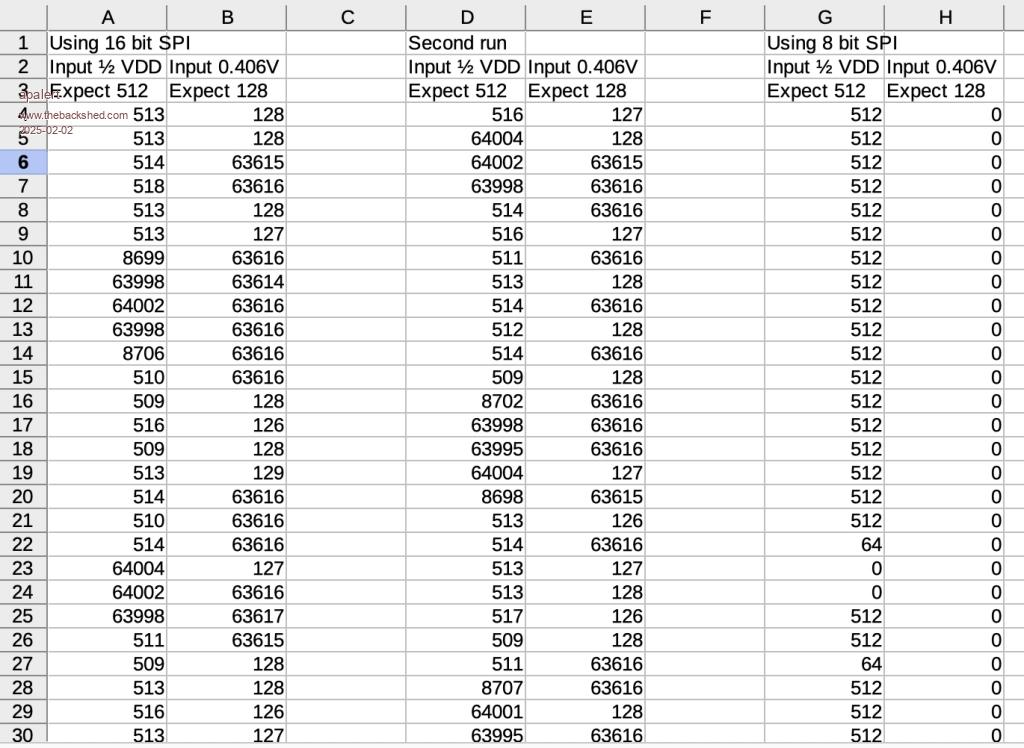 |
||||
| Pluto Guru Joined: 09/06/2017 Location: FinlandPosts: 375 |
I made a test program for MCP3004 some years ago. If I remember correctly it was ok. But I dont know if the operation is similar for your MCP3002. Please have a look and see if this makes any sense for solving your problem. 'FN1: option autorun on cls TEXT 160,40,"MCP3004","CM",1,5,RGB(white) TEXT 160,120,"10bit ADC","CM",7,2,RGB(yellow) TEXT 160,200,"FN 2021","CM",1,5,RGB(magenta) pause 1000 cls Dim integer TX,RX(2),HighByte, LowByte, i dim integer DOC 'Digital Output Code DIM float Vref=3.296, Vin, Avg, Vavg const CS=5 'Chip Select const DebugPrint=0 setpin CS, dout pin(CS)=1 pin(CS)=0 pin(CS)=1 'If the device was powered up with the CS pin low, it must be 'brought high and back low to initiate communication. ' bit|7| 6 | 5 |4 |2 |1 |0| 'TX=&b01000000' |0|StartBIT|Single/Diff|D2|D1|D0|0| D2 is 0 for MCP3004 TX=&b01000000' differential CH0-CH1 'TX=&b01000010' diff CH1-CH0 'TX=&b01000100' diff CH2-CH3 'TX=&b01000110' diff CH3-CH2 'TX=&b01100000' single CH0 'TX=&b01100010' single CH1 'TX=&b01100100' single CH2 'TX=&b01100110' single CH3 'The first clock received with CS low and DIN high will constitute a start bit. 'The SGL/DIFF bit follows the start bit and will determine if the conversion will be done 'using single-ended or differential input mode. The next three bits (D0, D1 and D2) are 'used to select the input channel configuration. 'If necessary, it is possible to bring CS low and clock in leading zeros on the DIN line 'before the start bit. This is often done when dealing with microcontroller-based 'SPI ports that must send 8 bits at a time. NOTE THE FIRST "0" IN TX! 'BY INSERTING ONE "0" BEFORE THE START BIT, THE OUTPUT MSB WILL START DIRECTLY WITH B9 'OF THE OUTPUT CODE. (No Null Bit before the Output Code.) 'The device will begin to sample the analog input on the fourth rising edge of the clock 'after the start bit has been received. The sample period will end on the falling edge 'of the fifth clock following the start bit. ' 'Once the D0 bit is input, one more clock is required to complete the sample and hold 'period (DIN is a “don’t care” for this clock). On the falling edge of the next 'clock, the device will output a low null bit. The next 10 clocks will output the result 'of the conversion with MSB first. do Avg=0 for i=1 to 100 MCP3004read Avg=Vin+Avg Next i Vavg=Avg/100 TEXT 160,40,"V="+str$(Vavg,1,4)+"V","CM",7,2,RGB(white) loop end' sub MCP3004read spi open 1000000,3,8 '8 bit mode 'Data is always output from the device on the falling edge of the clock. 'Mode 0,0 or 1,1 are possible. PIN(CS)=0 SPI WRITE 1,TX SPI READ 2,RX() if DebugPrint=1 then Print "RX0:";RX(0);" 0b";bin$(RX(0),8) if DebugPrint=1 then Print "RX1:";RX(1);" 0b";bin$(RX(1),8) 'Print "RX2:";RX(2);" 0b";bin$(RX(2),8) 'Print "RX3:";RX(3);" 0b";bin$(RX(3),8) HighByte=RX(0) and &b11111111 'B9:B2 of the output data HighByte= HighByte<<2 LowByte= RX(1) AND &b11000000 'B1:B0 of the output data LowByte=LowByte>>6 if DebugPrint=1 then print "HighByte";HighByte if DebugPrint=1 then print "LowByte:";LowByte DOC=HighByte+LowByte if DebugPrint=1 then Print "Code:"; DOC Vin=Vref*DOC/1024 if DebugPrint=1 then Print "Vin=";Vin PIN(CS)=1 'The CS/SHDN pin must be pulled high between conversions. spi close end sub Pluto |
||||
| TassyJim Guru Joined: 07/08/2011 Location: AustraliaPosts: 6266 |
I forgot to mask off the higher bits in the 16bit code data0 = data0 AND &h3FF etcdoing that will get rid of the obviously wrong readings. In the 8 bit version I should have masked of bits for each SPI read before adding them together. For some reason the second call to SPI2() is returning zero This is why the v/2 readings are too constant at 512 and also why the 0.4V reading is 0 instead of ~128 @Pluto the MCP3004 is very similar but has a couple more configuration bits so needs 17 cycles or 3 bytes. Edited 2025-02-03 13:18 by TassyJim VK7JH MMedit |
||||
| apalert Newbie Joined: 06/07/2023 Location: AustraliaPosts: 31 |
Jim, did as you suggested and you have nailed it! Results are amazing. Initially results were +/- 3. However I stabilised VDD on the VDC at 3 volts with an LM4040 and forced Pico into PWM mode while reading, now we get +/- 1 as per spec sheet. Was able to remove all pauses and bring clock back up to 1000000. Time to take 20 readings around 7.5m/s when not printing result of each loop. Hard to say which is better, 8 bit SPI or 16. Accuracy seems the same. 16 bit is a tiny bit faster. Thanks so much for your input. 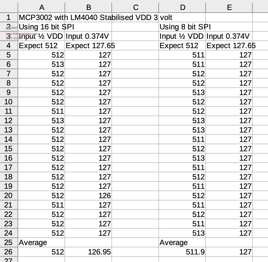 |
||||
| PhenixRising Guru Joined: 07/11/2023 Location: United KingdomPosts: 1333 |
Nice...and an interesting thread  |
||||
| The Back Shed's forum code is written, and hosted, in Australia. | © JAQ Software 2025 |
