
|
|
Forum Index : Microcontroller and PC projects : picoStretch RP2350B dev board
| Author | Message | ||||
| jvanderberg Newbie Joined: 06/05/2026 Location: United StatesPosts: 25 |
This is no-compromises RP2350B dev board that breaks out all 48 GPIOs. It's inspired by the Pimoroni Pico LiPo 2 XL W, which still supports the original 40 pin layout of the 'classic' Pi Pico boards. I think the pimoroni board does way too much, and I am not sure why it has castellated edges, because it's got chips on both sides, it can't be soldered down. My goals for this version: - 16MB Flash / 8MB PSRAM (CS GP0) - Expose all 48 GPIOs with castellated edges (a common nit with previous versions) - Support the original Pi Pico footprint for the first 20 pins on either side - USB-C / Radio Module 2 - Everything on the top side so it's solderable (there are solder jumpers on the back side) - Try to keep trace routing sane with not too many vias. I haven't sent this version to production yet, and am looking for feedback. I have made PCBs based based on the same schematic but with a different PCB layout, and it all works. I have one in my PicoCalc right now. You can find the kicad files here: https://github.com/jvanderberg/pico-stretch2. It's a 4 layer board with Inner1/Inner2 as ground planes. This helps with signal integrity and EMI for the traces that do have to move from the front to the backside. Definitely would appreciate feedback before I send this off to production. 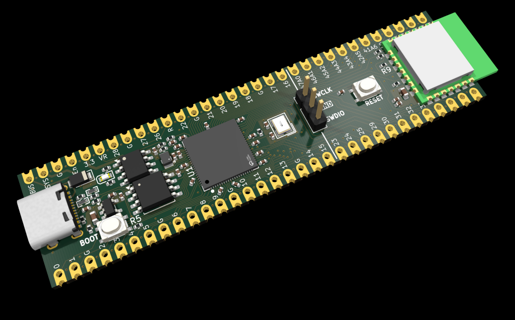 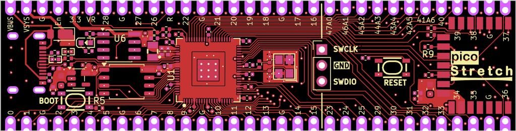 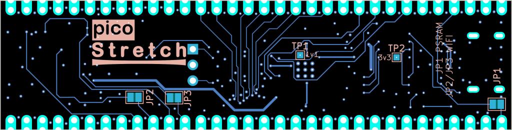 |
||||
| javavi Guru Joined: 01/10/2023 Location: UkrainePosts: 555 |
Please make the PSRAM CS signal configurable via solder jumpers, at least between GP0 and GP47. And route the USB signals to the contact pads on the underside of the board near the connector. Edited 2026-05-19 04:54 by javavi |
||||
| jvanderberg Newbie Joined: 06/05/2026 Location: United StatesPosts: 25 |
I'll think about the first, it might be pretty hard given the layout, but there's still a lot of freedom once you get to the backside. The USB pads are a good idea, I think that should be easy. |
||||
| javavi Guru Joined: 01/10/2023 Location: UkrainePosts: 555 |
I wasn’t able to view the schematic; if possible, please export it in an accessible format. Preferably, the radio module should not use any of the ports of the original Pico module. Pay attention to the quality of the components in the chip’s power circuitry. With proper core power, the RP2350 chip is capable of operating at 504 MHz. Edited 2026-05-19 05:34 by javavi |
||||
| jvanderberg Newbie Joined: 06/05/2026 Location: United StatesPosts: 25 |
I posted the link to the full KiCad repo, that’s got everything. Images of schematics on the web just tend not to turn out well. My existing boards based on this same schematic are pretty overclockable. I think you just have to get the 1v1 inductor right, and they basically hand hold you through the proper layout and give you the exact part they bless. |
||||
| bfwolf Senior Member Joined: 03/01/2025 Location: GermanyPosts: 244 |
I agree with you!  AFAIK GP0 is default for SPI0_RX or UART0_TX in PicoMite (don't remeber exactly). Pimoroni-Pico+2 also uses GP47 for PSRAM_CS. AFAIK GP0 is default for SPI0_RX or UART0_TX in PicoMite (don't remeber exactly). Pimoroni-Pico+2 also uses GP47 for PSRAM_CS.@jvanderberg: Many compliments and thx for your "Portable MMBasic" !!!  Perhaps you achieve by AI-help to add loadable DLLs to MMBasic (e.g. on PicoMite)?  I wrote several suggestions about this in the forum. Peter didn't like it..  A nice method would be the one used in the old MS-AmigaBasic.. If you have questions about: Feel free to ask! Regards, bfwolf |
||||
| jvanderberg Newbie Joined: 06/05/2026 Location: United StatesPosts: 25 |
Can you explain the use case? |
||||
| The Back Shed's forum code is written, and hosted, in Australia. | © JAQ Software 2026 |
