
|
|
Forum Index : Microcontroller and PC projects : TZBlox MCU32MX795 Final? review
| Author | Message | ||||
| MicroBlocks Guru Joined: 12/05/2012 Location: ThailandPosts: 2209 |
Phew, That was a long night (it's actually almost 20:00 here) , thinking, drawing, changing, etc. I think i have come up with a good design for a module. If you read the other topic you will know what kind of changes are done. Most important was to find a form factor that can be used in many cases. Because of the number of pins in case of a mcu module the choice has been made to use 1mm headers. All pins are available. For other blocks the number of pins are much lower. Most of the Blox are using I2c or serial, so just a few wires. This is the 3d rendering of the top the size is 29.5mmx29.5mm!: 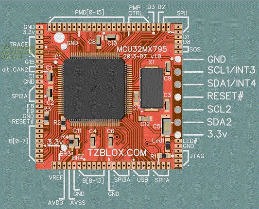
The most interesting change made from the previous version is the inclusion of pins on a 0.1" grid. This will allow quick connections, even on a breadboard. I show later in this post where this really shines. The pins are all on one side and they will be the same on all Blox. All these lines can be shared like a bus. There are two I2C busses, the idea is to use one as a slave and the other as a master so that communication between modules is extremely easy. A reset line for letting other blox know the system has been reset or a specialized Blox that can assert a reset under certain conditions. Watchdog anyone? :) The bus also has power lines, in this module only GND and 3.3v are used but there are two more lines possible of which one will have 5v and the other can be made project specific. The size of the module allows 11 pins on a 0.1" grid to be place on one side. To see the pins more clearly here is a rendering of the bottom: 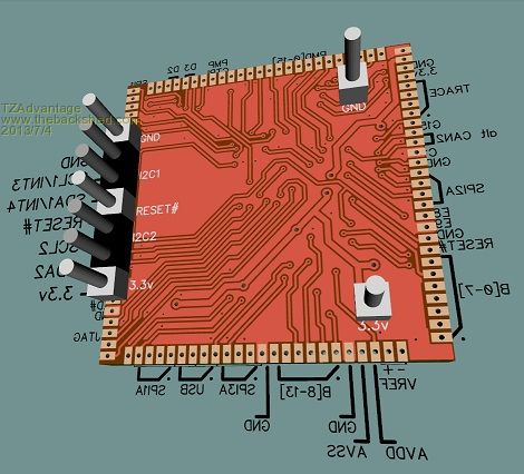
As an example how these Blox can be used i imagined a project that uses several of them. The imaginary project is a control system for aquaponics. It will need 3.3v regulated, a microcontroller, 8 analog inputs, 8 relays via optocouplers to electrically isolate them the controller, 16 io ports to read overflow switches, a display and a usb SD card. I then sat done and used Blox to assemble the system. (Blox shown are still in development, it is a proof of concept.) Within 30 minutes i made the 'schematics' consisting of blox and with measurements it can be made on a 10x15 centimeter carrier board. As you can see on the next drawing the carrierboard just has a few bus lines and for the more demanding blocks interconnections. Blox are design that the bus goes from left to right, interconnections are at the top and output at the bottom. As in the picture you can loop the bus around so that the interconnections face eachoter saving lots of traces. 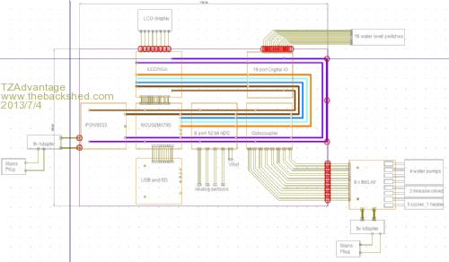
Here is the link to a better resolution: http://tzblox.com/Documents/_TZBlox_/MCU32MX795 As everything is contained in modules it allows you to bring to market products very quick, it will be very service friendly and easy to upgrade or expand. And don't forget, one of the concepts of Blox is that you use those modules in protoype friendly enclosures with header pins for easy connections. After you get it to work on your desk, it transfers seamlessly into a real quality end product. This is getting very close to a product, so if anyone has some remarks, now is the time to make them. :) A special thanks to JohnS, Stoveman, paceman and others for the invaluable feedback! Microblocks. Build with logic. |
||||
| Dylan Regular Member Joined: 17/06/2013 Location: NetherlandsPosts: 81 |
Is there a reason for the 100 mil offsets between the two pairs of GND and 3.3v lines? I can imagine space is an issue, but two extra "lanes" out of your 11 could be reserved for something else using stripboard. For documentation purposes, keep the ranges (like PMD[0-15]) [low-high], and I see that you have used a diagonal dot notation for order. I'd guess this is the low end, so perhaps just add an annotation to Top.jpg? Also I see you have X1 (8MHz) but I'm missing X2 (32768Hz) for RTC. What is lovely about your plans (and Kon's similar yet very different ones) is the tiny form factor. However, that isn't always an issue - as your 10x15 example shows. Nice :) |
||||
| MicroBlocks Guru Joined: 12/05/2012 Location: ThailandPosts: 2209 |
Thank you Dylan for the review. Yes the tiny form factor allows you to 'compose' a solution while still remaining relatively small as an end product. There is one more step in the Blox concept and that is instead of plugging the modules on a 'bus' you place the footprint and routings of the modules directly on the copper. This will make it even smaller and if a product needs high volume that is the ultimate way to go. There is something to say for keeping it in the form of modules though, because you then keep an upgrade and expansion path open, which can be a selling point. Costs and volume will probably force that decision when it is time to market your product. Kon's product has lots of merits too, and it can be a good mix. I have another 'backplane' board idea that i am working out. If that idea works out it could lift the whole concept to a new level of easy use and mixing modularity (sp) with project specific circuitry. I'll get back on that later. Microblocks. Build with logic. |
||||
| paceman Guru Joined: 07/10/2011 Location: AustraliaPosts: 1328 |
Hi TZ, I think the inclusion of the 0.1" pins and keeping them at 0.1" spacing with the other two on the board is a great idea - especially for ease of development. One thing I'm wondering. I presume all the 0.1" pins are solderable because the renderings look like they're not. They would need to be to allow them to be mounted on a breadboard, and the size of the holes would need to accommodate whatever the standard pin size is for breadboarding. Greg |
||||
| MicroBlocks Guru Joined: 12/05/2012 Location: ThailandPosts: 2209 |
Greg, All the pins on the 0.1" grid have standard header pin size holes. So yes, you can plug it into a breadboard. And what Dylan mentioned using a stripboard is great. Just solder a few female headers on it and you can plug them right in. I have changed the layout slightly by moving the left GND and 3.3v pins on the same 'lane' as the others on the right. Also i use the top left 0.1" grid pin as the home location. The 1mm grid pins start with the top left on -100,-250 mils. This will make it easier to draw a footprint when you want to make your own carrier pcb. I almost ready with the footprint, and i include it here shortly. [Edit] Added footprint. 
Microblocks. Build with logic. |
||||
| Dylan Regular Member Joined: 17/06/2013 Location: NetherlandsPosts: 81 |
Since you went from 900 mil to 1000, which is not a problem for I2C on a breadboard, perhaps the standard "host" should always have 2 pins 100 mil east from the power lines on the left. 1000 mil-wide modules would still be able to use both I2C channels, but potential future 900 mil-wide modules could use (11-2)x2 = 18 data channels of some description or another. Perhaps two fewer if 5V is reserved as a main bus (useful for servos). |
||||
