
|
|
Forum Index : Microcontroller and PC projects : Special "Back Shed" offer on Autotrax DEX
| Author | Message | ||||
bigmik Guru Joined: 20/06/2011 Location: AustraliaPosts: 2870 |
@MB, All, It appears that I am INCORRECT (not for the first time and certainly not the last) about the PCB, In fact it is by design that Iliya has it as a section of the Part itself.. It allows you to define a specific PCB shape including holes, cut-outs and copyright messages see the attached pictures (and part associated with it) for an example PART called Micks-Card .. PS. Iliya has chosen not to post here as he manages his DEX forum and that is the main point of support but he has offered these answers, (via email to me) in response to items mentioned on TBS.. Quote from Iliya.. --------------------------- Response to question on Back Shed. In the part editor, if you modify the PCB outline and select Use PCB border then when you place the part on a schematic, the PCB border if set from the part. This allows you to do parts with required profile. e.g. a Eurocard PCB with connector! Add holes, cutouts etc. Even import 3D. See attached part. Drag onto a schematic. Regards Iliya Kovac 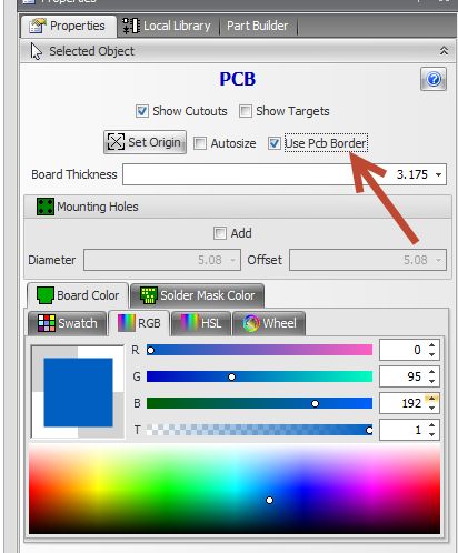
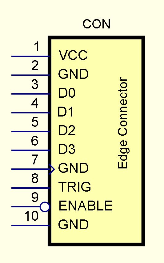
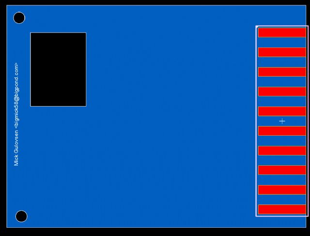
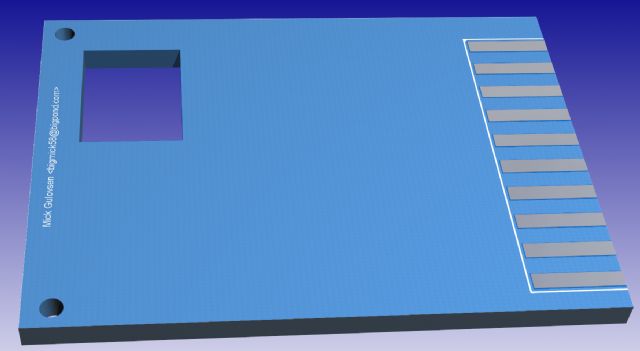
The part itself "Micks-Card" project file 2016-05-02_231732_Micks_Card.zip Regards, Mick (For Iliya) Mick's uMite Stuff can be found >>> HERE (Kindly hosted by Dontronics) <<< |
||||
| bigmik Guru Joined: 20/06/2011 Location: AustraliaPosts: 2870 |
Hi All, Another example of using the above part (Mick-Card) in a project with a few other parts added. 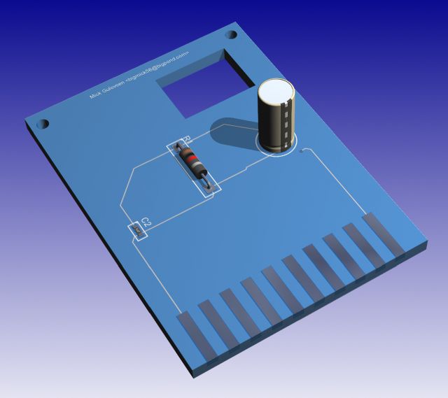
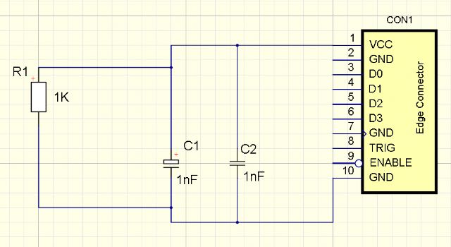
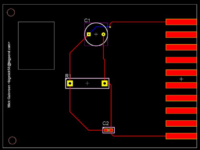
2016-05-02_232919_project.zip Kind Regards, Mick (for Iliya Kovac) Mick's uMite Stuff can be found >>> HERE (Kindly hosted by Dontronics) <<< |
||||
| bigmik Guru Joined: 20/06/2011 Location: AustraliaPosts: 2870 |
Hi All, Another answer from Iliya, Mik ---------------- Answer to question. In part edit the PCB autosizes unless you resize it and then its fixed. 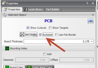
Regards Iliya Kovac Mick's uMite Stuff can be found >>> HERE (Kindly hosted by Dontronics) <<< |
||||
| bigmik Guru Joined: 20/06/2011 Location: AustraliaPosts: 2870 |
Hi All, Mick back in control of his body again.. 
All of the above shows that Autotrax DEX has a lot of complexity IF YOU CHOSE TO USE IT As Mentioned I have been using DEX for about 2 years now and didn't know some of these things, This thread has been a learning exercise for me as well. In truth once I worked out how to use the basics of DEX that is all I really needed.. But the above example could have saved me a bit of time and effort if I had investigated further, for example I have several `plug in boards' that are designed to have 3 x female headers on the under side of the PCB to plug into MuP these headers (and the size of the PCB) all need to be specific sizes and in specific places else they wont align properly onto MuP's male header pins.. I have, until now, ALWAYS had to carefully position these headers and resize (and position) the PCB manually, then LOCK them so they cannot accidentally move, every time I start one of the projects. I could have just created a part with PCB area defined and headers fitted and called it MuP-Plugin.part. I will do next time that situation arises. In fact when I did MuP I didn't LOCK my headers in and somehow I accidentally moved header J3 down 0.025".. It should have been on a standard GRID line alignment with J4 & J5 and that has caused me a headache since with having to check again the size and position of these headers before I actually start having fun laying out my new project. But then MuP was my very first Project I created with Autotrax DEX and as I have sold/given away around 500 MuPs I think we can agree that it certainly seems to be successful. Kind Regards, Mick Mick's uMite Stuff can be found >>> HERE (Kindly hosted by Dontronics) <<< |
||||
| MicroBlocks Guru Joined: 12/05/2012 Location: ThailandPosts: 2209 |
I feel dumb, because i can not move a trace that is on the bottom. Also changing the visibility of Top copper hides the pads from a part that is on the bottom. The traces stay but the pads are gone. There is also no silkscreen on the bottom. Traces on the bottom can not be moved, only the top traces. The part on the bottom i can not move (did i lock it somehow?). I must do something wrong (moving traces on bottom and top should be working from version 0.1, right?) but it got me completely stumped. 2016-05-03_052109_U2SP.zip Microblocks. Build with logic. |
||||
| bigmik Guru Joined: 20/06/2011 Location: AustraliaPosts: 2870 |
Hi Jean, You have PCB FILLED checked.. See this screen shot of lower RHS of screen (at the bottom of the L:AYERS panel 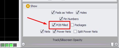
Regards, Mick Mick's uMite Stuff can be found >>> HERE (Kindly hosted by Dontronics) <<< |
||||
| MicroBlocks Guru Joined: 12/05/2012 Location: ThailandPosts: 2209 |
Yes, that solves the problem partially. But is that how it should be, it feels like it is a hack to solve a bug. I still can move tracks and parts on the top when i have the bottom current???? Would that not be unintuitive? Working on the bottom should keep everything on top undisturbed (unless you move a via of course). I also have a trace between pin 2 and 4 of the regulator (on the top) but can not draw traces on the top because the yellow net is not visible, they are on the bottom??? I know i have to get used to things but the above is counter productive as now i have to be super careful to not accidentally move a trace on the other side. I can make the layer i am not working on invisible, but then i don't know where the pads on the other side are. Is this really how it works, or am i doing something dumb again. Because that is what i feel at the moment. Microblocks. Build with logic. |
||||
| bigmik Guru Joined: 20/06/2011 Location: AustraliaPosts: 2870 |
@MB, I only check FILL PCB when I am finalising my silkscreen overlay as it makes everything very clear ... As to both layers visible and editable .. What is wrong with that? If I am routing manually I want to see every track on all layers (well at least top and bottom) to try to work out the best route, you can always uncheck to make any layer non-visible then you cannot see them, I do this when I am tidying up as I need to push and shove traces. Yes I can see the NETS disappear when the bottom layer is turned off, that never used to happen, it looks like it might be a bug in the recent download, I just found I can work around that by checking the make documentation layer visible. I will pass that onto Iliya Kind Regards, Mick Mick's uMite Stuff can be found >>> HERE (Kindly hosted by Dontronics) <<< |
||||
| MicroBlocks Guru Joined: 12/05/2012 Location: ThailandPosts: 2209 |
If i have parts on both sides and traces on both sides it gets very crowded, so much so that it would be impossible to select the right track unless you zoom in a lot. I would prefer that i can move things around only on the current layer and not accidentally (it are little mouse movements after all) move a trace a tiny bit on the other layer. In my case also the silkscreen did not show on the bottom and i think the reason the nets disappear is that the nets all originate from the QFN part that is on the bottom. I expected the nets to be always visible independent which layer is current. Microblocks. Build with logic. |
||||
| bigmik Guru Joined: 20/06/2011 Location: AustraliaPosts: 2870 |
@MB, All, Hi Jean, I see now that you are active in The DEX Support Forum and I have to ask that we try to keep questions on support/possible improvements etc kept in the appropriate area.. I am just a simple user (some say I am just SIMPLE). I am always happy to help you or anyone else who is having difficulty or in other ways.. I think Iliya emailing me and me reposting is not the best approach and after all the context of this thread is Special Offer on Autotrax DEX.. If there is enough interest maybe Glenn will offer an Autotrax DEX forum.. But Really as there is an active DEX forum should we re-invent the wheel. Anyway..... There is now just 3 1/2 days left for the Offer in case anyone is considering it.. It really is a good deal and a saving of $60 off the current price for DEX. Deal closes 7th May UK (GMT??) time. Kind Regards, Mick Mick's uMite Stuff can be found >>> HERE (Kindly hosted by Dontronics) <<< |
||||
