
|
|
Forum Index : Microcontroller and PC projects : DS18B20 and Hall effect sensor interface
| Page 1 of 2 |
|||||
| Author | Message | ||||
| Paul_L Guru Joined: 03/03/2016 Location: United StatesPosts: 769 |
I need to interface 14 DS18B20 temperature sensors and 2 Hall effect water flow sensors to PIC i/o pins in an electrically noisy environment over a distance up to 20 meters. If I power the sensors from 5vdc the hi level of the data line will have increased head room above any noise voltages which are coupled into the long transmission lines. But the PIC input pins I want to use (especially for counting the Hall sensor pulses) are not 5 volt tolerant. Can I clamp the signal voltage to 3.3v using a zener diode like this? Are these appropriate values? Paul in NY 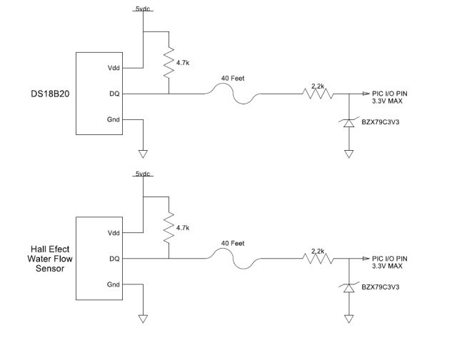 |
||||
| Zonker Guru Joined: 18/08/2012 Location: United StatesPosts: 772 |
The only way is to try it... As long as the pin gets pulled low enough, it should work... Hey, it's only 40 feet... These IC were suppose to do this medium length bus stuff..  |
||||
bigmik Guru Joined: 20/06/2011 Location: AustraliaPosts: 2981 |
Hi Paul, Zeners have a horrible drop off curve and as such are not suitable for Analog (not saying you want Analog) will probably be OK for Digital signals but you might be better off using 1N5817(or1N5818/9) pulled up to 3v3 as a clipping circuit. The max voltage at the PIC pin should be no more than 3v6 (lower with the 5817) which is within the voltage range the PIC can run at and through your 2k2 Ohm that would limit the current anyway. Such as: 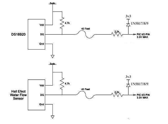 Regards, Mick Mick's uMite Stuff can be found >>> HERE (Kindly hosted by Dontronics) <<< |
||||
| Paul_L Guru Joined: 03/03/2016 Location: United StatesPosts: 769 |
Hi Mick, You're probably right about using a Schottky diode as a clamp. But I don't like putting more than 3.3v on the PIC pins. Would it be better if I used a series resistor and a zener on the 5 v supply to create a 3.0 v shunt regulator then clamp each PIC pin to that? This way the Schottky diode will avalanche at about 0.25 v so the PIC pin would be at a maximum of 3.25 v. Each Schottky diode will avalanche at about 1.1 ma so the total drain on the 3.0 v shunt regulator should be a maximum of 17.6 ma. The shunt regulator will operate at a nominal 25 ma so the 3.0 v should be stable under all conditions. Paul 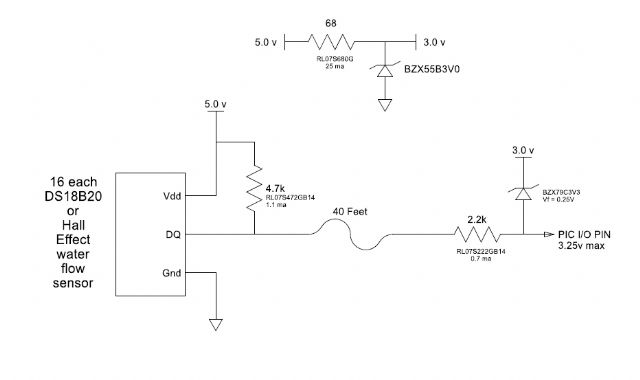 |
||||
Grogster Admin Group Joined: 31/12/2012 Location: New ZealandPosts: 9973 |
These are probably a good idea: Cheap bi-directional level shifters Those are the Chinese clone of the Sparkfun product here: SparkFun Level Shifter Thing They are very small, and will shift the levels either way - 3v3 to 5v, or 5v to 3v3. Smoke makes things work. When the smoke gets out, it stops! |
||||
| Paul_L Guru Joined: 03/03/2016 Location: United StatesPosts: 769 |
Whoops. That's the wrong part number for the Schottky diode in that schematic. It should have been the 1N5817! Paul |
||||
| WhiteWizzard Guru Joined: 05/04/2013 Location: United KingdomPosts: 2977 |
I would tend to agree with BigMik's suggestion; and there is certainly no issue with the low current clipped 5v input to the PIC. The only thing I would add is to try Mick's method in your 'noise' environment and check it works as you need. Solder a quick test circuit (do not use a breadboard!) and run it through a long length of cable with the 4K7 at the sensor end, and the limiter resistor and clamp diode at the PIC end. You may need to 'tweak' the value of the limiter resistor to somewhere between 1K and 10K - possibly depends on your 'noise'! Let us know what you end up trying/doing as this topic comes up a fair  WW |
||||
| Paul_L Guru Joined: 03/03/2016 Location: United StatesPosts: 769 |
@Grogster -- I think you're right! It just occurred to me that the DS18B20 interface requires data to go both ways. Clamping with the Schottky diode will only work with data going from the DS18B20 to the PIC pin. This thing uses a single N channel MOSFET with integrated diode transistor and two pull up resistors. It is based on a Phillips app note an97055.pdf and also on a newer NXP app note AN10441.pdf. I guess this is the way to go. Thanks everybody. Paul |
||||
redrok Senior Member Joined: 15/09/2014 Location: United StatesPosts: 209 |
You can make that level shifter with a single transistor. Here are some nice choices, there are many more.  You don't need the left resister as the PIC You don't need the left resister as the PIChas internal pull-ups. You choose the right resister. The basic advantage of using Depletion Mode MOSFETs and J-FETs (also depletion) is the gate can be grounded and 3.3V is not involved. Of course the standard way is to use Enhancement Mode MOSFETs as in the left circuit as in most of the shifter integrated circuits. BTW, in my test circuit with the J113 J-FET the source and drain were interchangeable. redrok |
||||
| Grogster Admin Group Joined: 31/12/2012 Location: New ZealandPosts: 9973 |
Hi redrok - nice to see you around the forums again.  I'm curious - if the DM MOSFET or JFET is actually a simpler idea(cos you can just ground the gate), why do they use the EM MOSFET in pretty much all the designs? Is it as simple as the fact that the EM MOSFET's are perhaps cheaper then the DM or JFET transistors? Smoke makes things work. When the smoke gets out, it stops! |
||||
| bigmik Guru Joined: 20/06/2011 Location: AustraliaPosts: 2981 |
Hi Paul, I really think that you are worrying over nothing, I have tried the clipping circuit extensively when I designed my MuP-Security circuit, (where I learned the folly of using ZENERs). I tried some voltages upto about 15v and the pic input never raised above 3v6 (in fact it was under 3v6 and I used 1N5819 diodes, the 1N5817 variety are supposed to be lower forward voltage drop ... Down to 0.1v) Of course those level translators Grogs suggested are dirt cheap and I have seen 8 channel ones so 2 of them should work perfectly for you.. Of course if you really DO have a noisy environment then maybe use some RS485 chips will work wonders for you.. You do NOT have to use these with a Serial uart .. They work well as level translators and are designed to work in noisy environments.. Mick Mick's uMite Stuff can be found >>> HERE (Kindly hosted by Dontronics) <<< |
||||
| redrok Senior Member Joined: 15/09/2014 Location: United StatesPosts: 209 |
Hi Grogster;I don't think its a cost factor, as the process for making Depletion Mode or DM MOSFETs is virtually identical. Just a matter of diffusion times and, I suppose, other things. Remember, they work in exactly the same way. It's just that they need extra voltage, to turn them off. J-FETs are the same way. They need extra voltage, to turn them off also. The primary reason there are a gillion EM MOSFETs is that when the gate voltage is zero the device is turned off. This characteristic is very useful. A second question is why are there no EM J-FETS. This is because they use a reverse biased PN junction so you would only have 1/2 a volt or so to switch from off to on. This is not enough for satisfactory gain. Historically, there were high power DM J-FETs but they completely vanished when MOSFETs appeared. Now J-FETS are mainly used in low power circuits. BTW, in the level shifters, I have found that the explanations of how they work is not precisely correct. They say the High voltage side pulls the Low voltage side down through the body diode. while this is is convenient to say, current is actually flowing through the MOSFET channel which is turned on. This current is flowing BACKWARD through the MOSFET NOT the diode. you can prove this with a scope and you will see the voltage across the MOSFET is much lower than a diode drop. Similarly, the J-FET example also works and has no diode. Even better, the source and drains are interchangeable. I wish MOSFETs didn't have a diode so their drain and source could be swapped. Unfortunately, the body diode is intrinsic to their structure. These do exist but I never had one. Apparently they are in some CMOS gates. redrok |
||||
| Paul_L Guru Joined: 03/03/2016 Location: United StatesPosts: 769 |
@Mick -- I don't think the clipping circuit will work with the DS18B20s powered by 5v. The clipping circuit is essentially one directional, from 5v to 3.3v. I don't think it will work when the PIC transmits the setup command from the 3.3v side to the 5v DS18B20 side to begin a conversion. @Grogs -- There's something wrong with the ebay link you supplied. Ebay level shifter The thing is supposed to transmit 4 channels but it only has 2 MOSFETs plus 4 resistors on the board. The other link Sparkfun level shifter is for a 4 channel and it has the expected 4 MOSFETS and 8 resistors. Sparkfun indicates that the circuit is of their design, but the two application notes from NXP both show identical circuits. NXP #1 and NXP #2 The NXP suggested design is definitely bi-directional and I suppose it would be best to use it. Since there are 20 sensors involved either 5 of the little Sparkfun boards will be needed, or 20 individual level converter MOSFETs will have to be wired on a special board which will also contain the connectors for the sensors. @jman -- Thanks for your alternate ideas of using two alternate MOSFETs and one JFET. Your ideas are much appreciated. As you pointed out, the pullup resistor on the 5v side can be eliminated because the PIC chip has internal pullup resistors. Paul in Poughkeepsie |
||||
| Grogster Admin Group Joined: 31/12/2012 Location: New ZealandPosts: 9973 |
The eBay ones only have two channels on the board, the SparkFun one has four channels per board. That is the only difference. Here are some eBay four-channel ones if you want them. Smoke makes things work. When the smoke gets out, it stops! |
||||
| robert.rozee Guru Joined: 31/12/2012 Location: New ZealandPosts: 2526 |
the data pin of the ds18b20 is open drain, see the below from the datasheet: 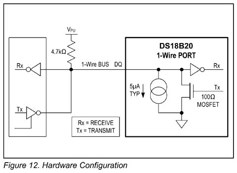 as such, there is no need for any level translation. the 4k7 pullup resistor, if connected to 5v, will provide insufficient current (less than 400uA) to in any way upset any of the micromite's 3v3 inputs. storm, teacup. cheers, rob :-) |
||||
| Grogster Admin Group Joined: 31/12/2012 Location: New ZealandPosts: 9973 |
...and there you have it folks. With that being said, I would be inclined to just forget the level-correctors completely. Are we in agreement? Smoke makes things work. When the smoke gets out, it stops! |
||||
| bigmik Guru Joined: 20/06/2011 Location: AustraliaPosts: 2981 |
Hi All, Not entirely, The biggest problem I see Phil having is 2 fold. 1. The length of the wire runs and, probably most importantly, 2. The NOISY environment that he plans to use these in. I really believe he needs to protect the PIC input pin from spikes and surges.. Quite frankly, it is now up to Phil to test his choice of the suggested options and see what happens. Where the noisy environment is concerned the RS485 transceivers with their `dual differential' circuitry `may' in fact be the only way to get a reliable signal across the length of cabling. How does RS485 help the signal integrity I hear you ask? It does this in two ways. Firstly the requirement to use a twisted pair cable minimises the effect of spikes (but not eliminates them). And secondly if a spike is induced into the pair from say a large generator or nearby welder etc. the same spike is induced in BOTH of the wires and as the circuit relies on the `difference' between the D+ and the D- this difference will be more or less the same with or without the noise as the same spike will appear in each wire of the pair. NOTE you do NOT need (and indeed should not have) a GND line between the Transmitter and the Receiver chip.. it is simply the 2 data wires. Anyway Phil, You need to try things out and see how you go. Kind Regards, Mick Mick's uMite Stuff can be found >>> HERE (Kindly hosted by Dontronics) <<< |
||||
| Paul_L Guru Joined: 03/03/2016 Location: United StatesPosts: 769 |
@Mick -- I ran across differential or balanced lines for broadcast audio circuits when I first got involved in broadcast engineering back around 1956. We used 600 ohm transformers with a grounded center tap feeding twisted and shielded pairs because we really wanted to avoid introducing a low level 60 cycle (that was before Hz) hum into the audio. In this single ended application if some 50 mv of 60 Hz hum is coupled into the data line I don't think it will be recognized as a level transition by the digital input gates. Furthermore, it will be bypassed to ground through the 4.7k resistor which terminates in a big tantalum capacitor. I am going to route these cables as far away from any motors as I can. The pumps are well shielded 1/6 Hp, the Freon compressor is 8 Hp but is encased in the hermetic shell and a steel cabinet. I doubt that I'll have any problem with 60 Hz hum or even switching transients. Anyway, thanks for worrying about me. @robert.rozee -- What is the input impedance of the sensor data pin and the PIC data pin when they are both HI? If the combined parallel impedance of both is 10k that would be in series with the 4.7k resistor. The voltage on the data line would then be 3.3 + (5-3.3)(10k/14.7k) or 4.46v and the current in the 4.7k resistor would be 1.7/4.7k or 362 ua. You are correct that this would not bother the PIC inputs. However, I want to try to keep the impedance of the path to ground through the filter capacitors as low as possible to attenuate any 60 Hz hum or switching transients which could be coupled into the data line. If I locate a level translator physically near the PIC pin then most of the 40 foot line will be at 5v when HI providing more head room above any induced garbage and the impedance to ground through the power supply filters will be (4.7k + Zc) probably less than 5k. This would result in a little quieter line than if the line were at about 4.46v as above. The whole decision hinges on the input impedance of the sensor pin and the PIC pin when they are at their HI state. I don't know if this spec is available. As you say, it might be a tempest in a teapot. Paul in Poughkeepsie |
||||
| robert.rozee Guru Joined: 31/12/2012 Location: New ZealandPosts: 2526 |
neither pin has a "HI" state as such - they are either pulled to ground (logic '0') by an open-drain mosfet, or high impedance (input/logic '1'). the impedance at the '1' state is dictated entirely by the 4k7 pullup resistor, a component that is essential for the bus to work. the value of this pullup resistor is dictated by the drive capability the ds18b20's data pin, and as such you don't have much leeway to change the value (at best, you may be able to halve it). being a bi-directional bus with direction outside of your control, the only real option is to either place a small micro with each ds18b20 in order to provide a more robust interface (rs485 or ttl rs232), or, to place your micromite closer to the sensors (or use multiple micromites). cheers, rob :-) |
||||
| Paul_L Guru Joined: 03/03/2016 Location: United StatesPosts: 769 |
Exactly what I thought Rob. When either the PIC pin or the sensor pin is in a high state its impedance to ground is very high, probably >> 1M, but neither pin can source any voltage. This means that the full 5 v from the 4.7k pullup resistor appears on both pins. A level translation circuit pretty much has to be provided near the PIC chip if a non 5v tolerant i/o pin is being used. At TTL levels any voltage below about 1.5 v will be recognized as LO while any voltage above about 3.5 v will be recognized as HI. The indeterminate range is 1.5v to 3.5v. If the input uses a Schmitt trigger then hysteresis will reduce the indeterminate range to 2.2v to 2.8v. Any noise voltage coupled into the long line will see a very high impedance >> 1M to ground when both pins are HI. Since the equivalent source impedance of this coupled noise voltage is very high ( >> 10M ) we should be able to attenuate the noise voltage by coupling it to ground through a resistor, 10k in this example. This produces a voltage divider instead of a pullup resistor and limits the HI voltage to 3.4v, but it would attenuate a 500 mv noise voltage with a source impedance of 10 M to 5 mv. If the PIC pin began drawing a current of 0.1 ma in the HI state that would increase the current in the 4.7k resistor to 0.34 ma and reduce the voltage applied to the PIC pin to 2.93 v in the HI state. Would you feel safe in applying this 3.4v HI voltage to a non 5v tolerant PIC pin through this voltage divider? Can any or all of the PIC pins be set to not source any voltage (open drain/collector) in MMBasic code? Paul in Poughkeepsie 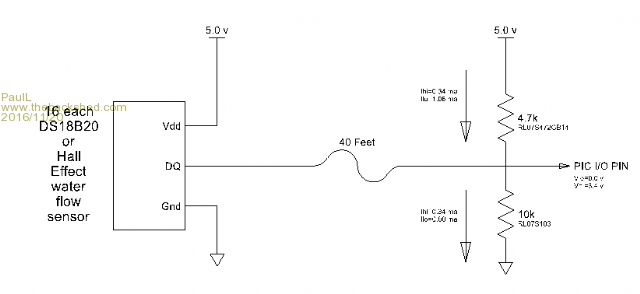 |
||||
| Page 1 of 2 |
|||||
| The Back Shed's forum code is written, and hosted, in Australia. | © JAQ Software 2026 |
