
|
|
Forum Index : PCB Manufacturing : A result that I cannot understand
| Author | Message | ||||
OA47 Guru Joined: 11/04/2012 Location: AustraliaPosts: 1050 |
I have been successfully creating CNC routed prototype PCB's for some time. Over the last week I have been experimenting with laying a solder mask over the routed PCB and the milling off the mask on the solder pads. I have not been at all successful and I cannot fathom the cause of the results. I am using K-CAD to generate the G-CODE for the job and using the electric sensing probe to set the tool height. I hope my problem is demonstrated with the attached picture. 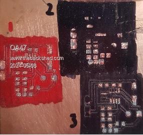 The red board has been isolation routed and as you may be able to see some of the pads have been completely cleared away and others are perfect. I used a 60 degree 3.125mm chamfer bit and my first thoughts were that the variations in the thickness of the PCB would cause this issue. The second attempt (labelled 3) is the lower black attempt that isolation routed ok, this time I used a 2mm conical bit and it shows generally the same pads being cut through although this is a newer area of the blank PCB. The G-code definitely shows the Z depth to be consistent over the job when I checked the code. The third attempt (black, labelled 2) was using a 0.1mm flat conical bit (no isolation routing prior) and again the pads previously destroyed are the same ones even when others are missed completely. I am at a loss to see what is happening here and how I can fix it. 0A47 |
||||
| phil99 Guru Joined: 11/02/2018 Location: AustraliaPosts: 3313 |
Unless you are planning on wave soldering these boards, it may be easier to wait until after the components have been soldered to apply the coating. That is how I have been doing it for half a century. |
||||
| greybeard Senior Member Joined: 04/01/2010 Location: AustraliaPosts: 181 |
Is the sensing probe optical? if so it might be 'confused' by the coating and/or a reflection. Edited 2024-05-03 17:57 by greybeard |
||||
| OA47 Guru Joined: 11/04/2012 Location: AustraliaPosts: 1050 |
Phil the reason that I want to have the solder mask is to prevent solder bridges when attaching the components. 0A47 |
||||
| OA47 Guru Joined: 11/04/2012 Location: AustraliaPosts: 1050 |
Greybeard, the probe sensing is electrical contact between the PCB and the tool. 0A47 |
||||
| phil99 Guru Joined: 11/02/2018 Location: AustraliaPosts: 3313 |
Fair enough. Doesn't help me though. I have a talent for bridging pins regardless and always have to finish with solder-wick on SMDs. |
||||
| OA47 Guru Joined: 11/04/2012 Location: AustraliaPosts: 1050 |
Sorry for the memory slip. This should have read. I am using Flat-CAM to generate the G-CODE for the job 0A47 |
||||
| SunBakedWA Newbie Joined: 22/12/2023 Location: AustraliaPosts: 6 |
Hi OA47, Did you use the same bed position for each of the solder resist removal attempts? Just thinking it might be a small amount of play on the mill axis resulting in very slightly too much Z travel in that area of the bed, or maybe the bed is slightly higher in that area? My thinking being Z axis zeroed OK so the tool tip height is the same, three different bits of copper clad board unlikely to warp in the same place and the G-CODE is correct for programmed Z height the only thing left that could vary is the actual machine... I wonder if you could edit the G-CODE to re-zero Z before the route on the first of the problematic pads, that way you will know the tool is just touching the copper before the actual routing operation takes place. It would be a pain but it could indicate if there is some sort of back lash going on as prior to the zero the Z axis DRO will indicate the difference between the previous zero and the current one. Another thing that might point at the problem is to run the clear off program after the isolation route without actually having the solder resist on or moving the board. Hope this helps SunBakedWA Everything here has been Sun Baked in WA |
||||
bigmik Guru Joined: 20/06/2011 Location: AustraliaPosts: 2981 |
GDay OA47, All, Most copper clad PCBs are 1oz which has only 0.035mm copper thickness. I don’t know what CNC you use is but that is about 1/3 of what most cheap CNCs quote for their accuracy. That aside, I am thinking that the bed may not be entirely flat, I would suggest that you clamp a sacrificial block to the table and mill it flat and secure your PCB to it. Make sure the other side of the PCB is smooth and free from dust etc. Then try your cuts. There is a fine line when we are talking copper that is only 35microns thick. I wonder if you could apply drips of wax to these spots before you apply the coating then by boiling the board you may be able to clear those areas. BTW I have just bought a new CNC to play with (old one is a standard 3018) a Genmitsu 3020 Pro Max V2. Which purports to be able to mill aluminium and brass. Not that I need to do that much but I like its rock solid stability and lack of backlash. I think the issue might be more that your table is not perfectly flat. Kind regards, Mick. (The big one) . Mick's uMite Stuff can be found >>> HERE (Kindly hosted by Dontronics) <<< |
||||
| OA47 Guru Joined: 11/04/2012 Location: AustraliaPosts: 1050 |
Thanks BigMik for your input. The CNC is a 30 X 40 unit I have built myself. I don't think that the bed levelling is the problem as I have milled it and ran the gauge over it and it seems to be better than 0.02 mm overall. As described the issue is that the same certain pads are affected in different areas of the milled areas. I have found a work around for the moment using a Dremel soft polishing bit but the tools wear quickly so I will be hunting for a better solution.  0A47 |
||||
TassyJim Guru Joined: 07/08/2011 Location: AustraliaPosts: 6541 |
I had good results using autoleveller. http://www.autoleveller.co.uk/ It will compensate for bed and PCB irregularities and tell you it is really flat. Jim VK7JH MMedit |
||||
| OA47 Guru Joined: 11/04/2012 Location: AustraliaPosts: 1050 |
Thanks Jim but as I have mentioned I do not believe that the issue is height levelling as the same pads are affected in different areas of the PCB blank. 0A47 |
||||
| SunBakedWA Newbie Joined: 22/12/2023 Location: AustraliaPosts: 6 |
Hi OA47 Just a thought, if its not the height of the bed and its the same pads in different places on the blank and we know the actual GCODE is correct then the copper foil must be higher in those pads than in the other areas as they would not be being milled away. So the question becomes what is making those parts of the copper foil be slightly higher? Is there any chance the etch resist may be causing the copper pads to lift slightly by soaking into the PCB backing (I would say G10 but I don't recall if you are using fiberglass PCB substrate) or causing the PCB to expand slightly and the affected pads are in board areas that are more exposed and thus more affected? Kind of throwing ideas now as you have eliminated other variables.... A test to see if its caused by the etch resist would be to run your pad clearing GCODE on a board that has not had the resist applied - if the same pads still get milled away then its not that! If they don't get milled away then apply the resist in your normal way and re-try. Just trying to suggest ways to break the problem down to eliminate possible causes. Good Luck  Everything here has been Sun Baked in WA |
||||
| The Back Shed's forum code is written, and hosted, in Australia. | © JAQ Software 2026 |
