Notice. New forum software under development. It's going to miss a few functions and look a bit ugly for a while, but I'm working on it full time now as the old forum was too unstable. Couple days, all good. If you notice any issues, please contact me.
Forum Index : Electronics : Inverter building using Wiseguys Power board and the Nano drive board
Page 43 of 43
Author
Message
KeepIS Guru Joined: 13/10/2014 Location: AustraliaPosts: 2286
Posted: 12:06am 14 Oct 2026
Copy link to clipboard
Print this post
Hi, it certainly sounds like they only want 1oz, I'm glad I got enough boards for my friend's build and my spares and one full backup Inverter as well, to be sure to be sure!
I'm going to use quality 3.3mm diameter copper with around 200° rating, in reality the only way to get smaller amounts is to find a motor winder or business with a partial drum to sell, or just bite the bullet and purchases a full drum.
As I'm helping a friend build three of your dual Inverter design, we have decided get a full drum and I doubt the cost will go down in the near future, it my even become almost impossible to get.
BTW, both of us are trying to stretch our budgets (who isn't these days?) and prices are going crazy (for everything)
Mike, would believe that I'm still working on finishing touches to the extension!
I was up on the roof of the big shed and carport yesterday, cleaned all the solar panels, roof, gutters, and the flush diverters for the W-tanks etc.
nickskethisniks Guru Joined: 17/10/2017 Location: BelgiumPosts: 499
Posted: 07:12pm 14 Oct 2026
Copy link to clipboard
Print this post
Yup crazy, last week I bit the bullet and ordered some extra pcb's. So if someone in Europe want's an extra board you can contact me. Components are getting expensive, I'm allways buying in bulk but that adds up verry quickly, capacitors at 4-5€ pcs after the the discount you get with buying 50pcs.
7-8y ago I had to buy a whole spool of 42.8kg 3.55mm enamelled wire, 562€, declaring myself crazy doing this. Now I think it was a good investment. 😁 I'm not looking forward to wind a new transformer though, but potted cores enough to dismantle first. 🙃
One moment I was really thinking about just buying some blue rubish, I would have had a nice system looking at all my investments, but then I came to senses real quick. Nothing is more fun then building and creating things yourself.
KeepIS Guru Joined: 13/10/2014 Location: AustraliaPosts: 2286
Posted: 11:17pm 14 Oct 2026
Copy link to clipboard
Print this post
Yes, and it's very satisfying especially building for off grid, and especially when the overall system turns out to be better than a commercial off grid system, and you can "EASILY" fix it if needed.
I would feel feel "extremely vulnerable" with good verified reasons, if relying on a commercial system.
Like you, I purchase parts in bulk in case the supply lines start to fail or become unaffordable, both are looming IMHO.
That was definitely the right thing to do getting that big reel of copper cable.
FYI: Received a phone call yesterday evening from a forgetful family member living a few km away, asking if we has also lost power, I reminded them that I would't know as I'm not connected to the mains, I had to look outside - and sure enough, total blackness.
With all the solar battery uptake over the past two years (big rebates), I thought I'd look out and see at least a couple of homes with the lights on, nope, nothing but total blackness as far as the eye could see, quite eerie looking out and seeing nothing but your own yard, feels like yours is the only home for miles, or everyone suddenly disappeared.
Apparently power has been going off randomly for a few minutes at a time over the past few months, last night it was off for around 7 hours, so I'm told, started right when most people were about to make the evening meal.
Looks like we are in for at least 5 days straight with no Sun and dark very overcast weather, we need rain desperately here, but it looks like a few sprinkles is all we will get out of it
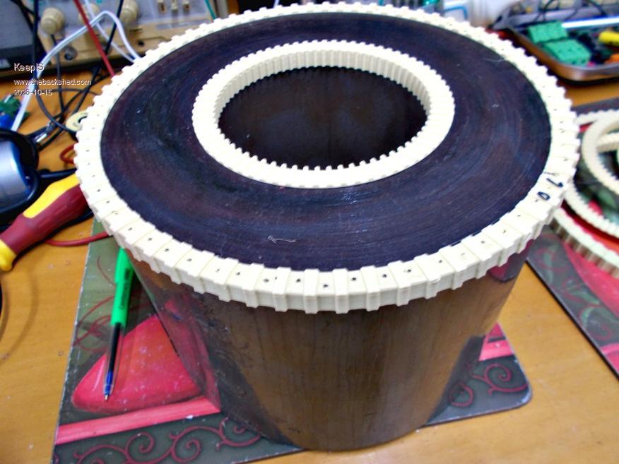
Test end caps on one end - final units will have a chamfer and be locked in place with epoxy. : Edited 2026-10-15 15:39 by KeepISNANO:Inverter V 8.4ks - Linux AvrDude GUI script V4.1
KeepIS Guru Joined: 13/10/2014 Location: AustraliaPosts: 2286
Posted: 04:07am 25 Oct 2026
Copy link to clipboard
Print this post
Solar & flood update: I'm guessing most in AU have seen the News pictures and weather we have been having over the past few weeks in SE QLD, day after day with no sun, dull overcast sky and rain, we had 18", around 455 mm in a day and a half at the peak, fortunately our property is higher and does not flood, although roads were / are flooded everywhere around here, still raining and overcast with another big front moving in.
Forecast is for a bit of sun in a day or so, with the possibility of real sunshine in 4 days.
We are very lucky to live in a location like QLD with the solar power we get here, even though the W/m2 Solar power has been in the toilet between 100 to 300 range, the batteries have not been below 52%, and that was after two days of < 120 W/m2, they are now sitting at 98% as the clouds cover has thinned slightly but rain is still falling, but we are ready for the next onslaught, our days & years of continuous off grid power keep increasing.
This, despite only having 8 panels north facing, the rest are flat or south facing.
South is the worst possible direction for this location, and once again shows that panels under full cloud cover do not care about angle or aliment as they all produce exactly the same power output under full overcast weather, and even then at this location, 8 panels mounted flat are almost as good as 8 north facing in full sun, and flat panels produce more output as the sun comes around to set in the west, the old saying of location, location hold true for most things.
My mate has another commercial Inverter blow today, that's 3 out of the four, we previously managed to fix two, sh*ts of things to work on. He is now building two of the Dual Inverters as fast as he can. : Edited 2026-10-25 14:10 by KeepISNANO:Inverter V 8.4ks - Linux AvrDude GUI script V4.1
Godoh Guru Joined: 26/09/2020 Location: AustraliaPosts: 715
Posted: 04:27am 25 Oct 2026
Copy link to clipboard
Print this post
Hi KeepIS. Well like you we never have blackouts. We got a bit of rain last night and today, which has been fantastic. Only around 25mm but more than for a while, it is pretty dry here, usually we live in a very wet area. But still with rain and fog all day we are still charged up to 100%. I was given a Selectronics Pro inverter a while back and decided to swap out my home made inverter with it in the last couple of days. Today I took the cover off it and saw what you mean about difficulty of repairing commercial inverters. Fortunately it works fine and I have my 4kw home made one as a spare. I am thinking of having a go at building a wiseguy power board and using the transformer in my home made inverter to update it. I have problems getting the aliexpress 8010 board current overload adjustment working properly. So maybe it is time to update it. With 43 pages to read though on this thread it may take a while though. cheers pete
KeepIS Guru Joined: 13/10/2014 Location: AustraliaPosts: 2286
Posted: 05:04am 25 Oct 2026
Copy link to clipboard
Print this post
Some of the bigger commercial inverters are just an exercise of torture to dismantle, good luck with getting a full official circuit.
There is no real need to read through the complete thread, there are two sections where I built the previous power boards and controller, and towards the end where I build the new Rev Power board and controller.
Then we have the WG Inverter Facebook group building a few as well, so any clarification you need can be asked here as it will help others, there are a few of us who have build them and would be more than happy to clarify things, or start another new build thread and we will happily clarify any thing needed.
Godoh Guru Joined: 26/09/2020 Location: AustraliaPosts: 715
Posted: 05:20am 25 Oct 2026
Copy link to clipboard
Print this post
hi KeepIS, I am not after a Selectronics diagram. It has a pretty decent transformer and inductor in it. If it ever died I would just use those bits and make a simple unit. It seems like a nice inverter but very complex. The home made inverter I have is the one I would most likely put a wiseguy board into. The Aliexpress boards have heaps of variations, so using the home made transformer and box with a wiseguy board would be a good option. I will read more about what you did Thanks Pete

 Notice. New forum software under development. It's going to miss a few functions and look a bit ugly for a while, but I'm working on it full time now as the old forum was too unstable. Couple days, all good. If you notice any issues, please contact me.


 Print this post
 and I doubt the cost will go down in the near future, it my even become almost impossible to get.