Notice. New forum software under development. It's going to miss a few functions and look a bit ugly for a while, but I'm working on it full time now as the old forum was too unstable. Couple days, all good. If you notice any issues, please contact me.
LadyN Guru Joined: 26/01/2019 Location: United StatesPosts: 408
Posted: 06:35pm 11 Mar 2019
Copy link to clipboard
Print this post
The Warpverter brain takes in DC power, say from batteries, rectified AC, PV Panels and the like and generates control signals for H-Bridges that drive transformer stages.
The Warpverter has a very unique design - it's actually composed of cascading inverters (hence StepInverter) that assemble harmonics of square waves to create a practically pure sine wave output.
The THD of the Warpverter decreases as we increase the number of cascades with each cascade handling less power than the previous in proportion to their harmonic coefficient.
Tony has implemented the brains using discrete digital gates, an ADC and an EEPROM.
The EEPROM data generation itself requires a separate thread because it's not very intuitive.
In this thread, we assume the EEPROM is available and programmed.
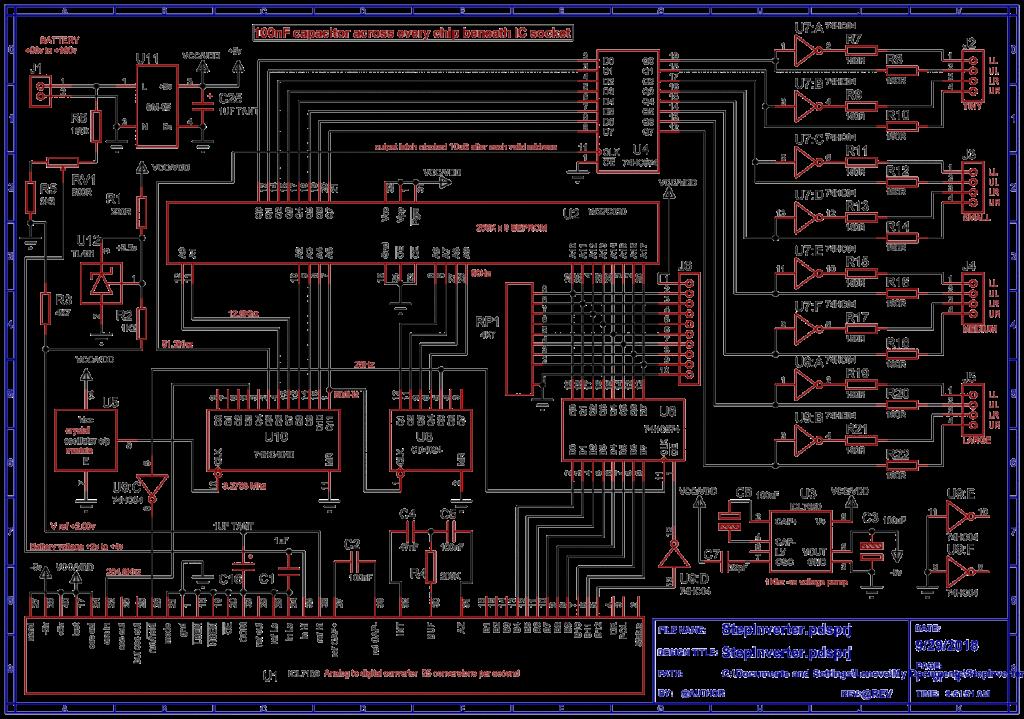
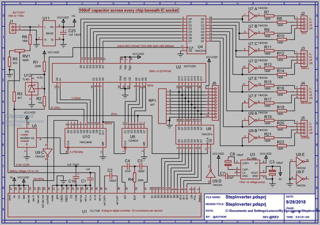
Here is a schematic of the Warpverter brain control board.
Below is an detailed post from Tony to explain how it works:
LadyN Guru Joined: 26/01/2019 Location: United StatesPosts: 408
Posted: 06:38pm 11 Mar 2019
Copy link to clipboard
Print this post
LadyN Guru Joined: 26/01/2019 Location: United StatesPosts: 408
Posted: 06:42pm 11 Mar 2019
Copy link to clipboard
Print this post
Edited by LadyN 2019-03-13
Warpspeed Guru Joined: 09/08/2007 Location: AustraliaPosts: 4406
Posted: 09:53pm 11 Mar 2019
Copy link to clipboard
Print this post
Natasha, thank you for starting a new thread. The above schematic for the control board did not come out very well, so here it is again.
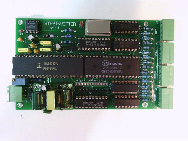
And here is the actual control board:
Just connect this up to the dc source, solar, battery, (or whatever) and it produces all the required mosfet gate drive waveforms for four inverters and provides voltage regulation without requiring any voltage feedback.
Edited by Warpspeed 2019-03-13Cheers, ĀTony.
hary Regular Member Joined: 15/04/2019 Location: FrancePosts: 89
Posted: 07:23pm 30 Apr 2019
Copy link to clipboard
Print this post
I wonder how's that possible ?
LadyN Guru Joined: 26/01/2019 Location: United StatesPosts: 408
Posted: 08:11pm 30 Apr 2019
Copy link to clipboard
Print this post
Tony meant line regulation and not load regulation of course.
For load regulation, voltage feedback will be necessary. No way around physics.
I of course don't know what I don't know.
Warpspeed Guru Joined: 09/08/2007 Location: AustraliaPosts: 4406
Posted: 09:03pm 30 Apr 2019
Copy link to clipboard
Print this post
Think of it like this Hary.
Suppose we designed an inverter that always feeds a constant ac voltage into the primary of a transformer. As the incoming dc voltage varies up and down, the inverter compensates exactly for these incoming dc variations ahead of the transformer.
If the load on the inverter stays exactly the same, the output voltage will remain perfectly constant in amplitude over a very widely changing dc input voltage.
If the load changes, the output voltage will fall very slightly with increasing load, mainly due to resistive losses in the transformer windings and the mosfets. The drop in voltage is not serious, and can be ignored for a practical real world inverter.
The interesting thing about this, is that the input voltage correction can act very fast indeed, and be completed in one very swift correctional step. If the shift in gain is carried out right at the zero crossing point, there will be no disturbance to waveform continuity, even for massive voltage corrections.
With voltage feedback, the inverter output voltage HAS TO ACTUALLY FALL before correction can even begin. Correction then has to be fairly gradual, to prevent any over correction, which will definitely lead to instability problems.
Its also a lot easier to measure a dc voltage quickly and accurately. An ac voltage is constantly varying over each cycle, so rectification and some averaging (smoothing) is required, all of which is SLOW and further adds to the feedback response time.
So the input voltage correction scheme is very fast, accurate, and requires fewer parts. There will be some small residual output voltage error that changes with inverter loading, and there are ways to get around that.
The extra parts count and complexity are arguably just not worth the trouble. The grid goes up and down in voltage all the time, and everything works just fine.
What is more objectionable is light flicker during sudden step load changes, and what is needed is very rapid speed of response to load changes, rather than always having a precisely exact output voltage.Edited by Warpspeed 2019-05-02Cheers, ĀTony.
hary Regular Member Joined: 15/04/2019 Location: FrancePosts: 89
Posted: 09:37pm 30 Apr 2019
Copy link to clipboard
Print this post
All this make actually lot of sense indeed !
Thanks for all the detailed explication !
That wouldn't have been my chosen route at first sight.