
|
|
Forum Index : Electronics : Mack-OffGrid’s 26.5 Volt Warpverter
| Author | Message | ||||
mackoffgrid Guru Joined: 13/03/2017 Location: AustraliaPosts: 460 |
All my PCB's are only 1Oz. According to my calculations they should be fine. 12v is fine if you use TLP250 or that other Opto driver someone found. The MIC4420 will work at 12V also. RS does have the MIC4420 and the IR4420. There are other PIN equivalents like the heavier TC4452 (its not required). MIC4420 AliExpress Just the first one I found - I haven't bought from here. I am using 15V parts in those little DCDC converter - mainly because I have a mixture of optos. Not all your driver Boards will need the MIC4420. 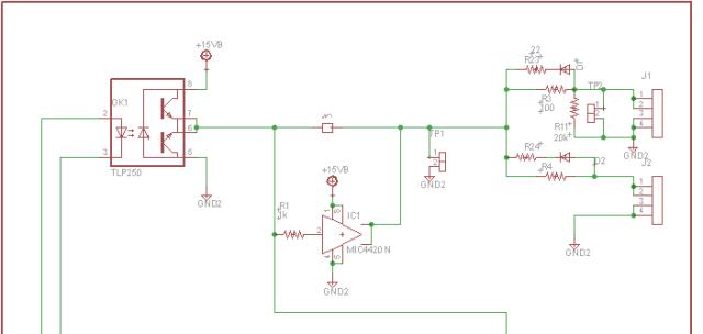 If on a given Full Bridge driver board you have no intention of expanding to Half Bridge Boards then you only need the Opto Driver and place the Jumper on, and leave the MIC4420 out altogether. The Half Bridge boards obviously need the '4420s. J11, the 12 pin IDC in the middle of the board can be omitted unless you intend to use it - and the 2 pin testpins TPx can be omitted - I used them for quick access for my CRO probe (I've made a cro lead going to a 2pin socket) The 100k SMD pulldowns on the Mosfet board aren't necessary as there are pulldowns on the driver board. However if you power up without the driver board the FETS will likely blow. They are a larger SMD (1206) and should be able to hand solder it. (none of my Mosfet boards have these pulldowns - just thought it was a good idea) Cheers Andrew |
||||
renewableMark Guru Joined: 09/12/2017 Location: AustraliaPosts: 1678 |
Thanks mate, if you type it with the "N" at the end nothing comes up, had me stumped  Cheers. Cheers Caveman Mark Off grid eastern Melb |
||||
| mackoffgrid Guru Joined: 13/03/2017 Location: AustraliaPosts: 460 |
Full Bridge Driver Board - Assembly - Omit these Parts - Optional - Include Part The 2 pin headers labelled as TPn are test points and are also optional. Standalone 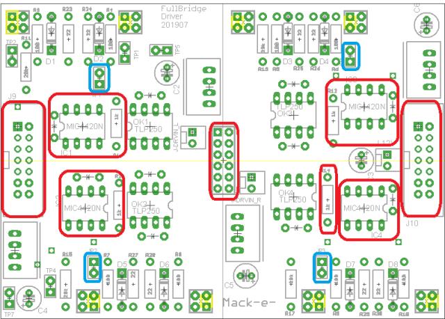 Driver Connected to Half Bridge Boards If the small B1215 PSUs are used on the half bridge boards it would be advised to also install them on the Full bridge Boards. 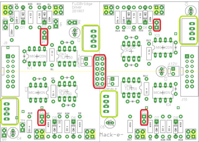 Cheers Andrew |
||||
| renewableMark Guru Joined: 09/12/2017 Location: AustraliaPosts: 1678 |
G'day Andrew, where you say jumper, you mean to short those two pins, so I could just solder in a wire across them yeah? Cheers Caveman Mark Off grid eastern Melb |
||||
| mackoffgrid Guru Joined: 13/03/2017 Location: AustraliaPosts: 460 |
yes indeed. |
||||
| mackoffgrid Guru Joined: 13/03/2017 Location: AustraliaPosts: 460 |
Tidy up - Front Panel I am not by nature a tidy person. All the wires leading to and from the Front panel were very untidy and apt to get tangled up etc. My solution was to make a front panel PCB and a rear panel PCB. 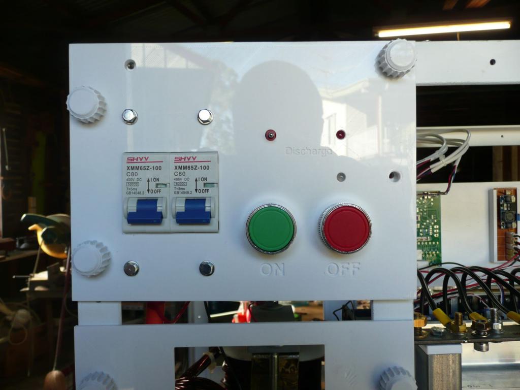 The Front panel has the Charge - Discharge Toggle switch, Bi-LED for Charge / discharge, ON and Off push buttons with a Bi-Red-Green-LED for inverter State, and a Buzzer. It was a real mess. So now the 2-way toggle switch, the two Bi-Leds and the buzzer are PCB mount. Power from either side of the circuit breaker are feed into the pcb along with the two push buttons switches. 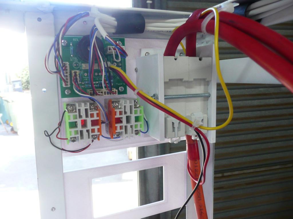 I then run power and signals back to a rear panel PCB which has the Charge - discharge resistors, 12V power supplies for the WarpVerter electronics and 12V to feed the isolated power supplies. 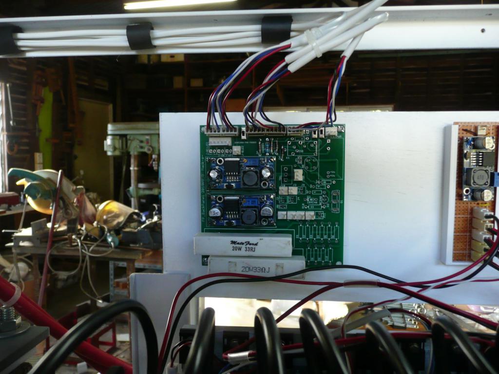 This back panel PCB can take the LM2596 power supplies like I have done but can also take the ACDC power supplies. I've got the circuitry there to test an active charging circuit for the 100+Volt inverter. There's a jack to provide for Fan power. I've also included some small switches and jacks for testing purposes. I haven't tested all the modes yet but I'll put these PCBs on Github when I'm satisfied. Very pleased with the tidy up, Cheers Andrew |
||||
| Warpspeed Guru Joined: 09/08/2007 Location: AustraliaPosts: 4406 |
Haha, I know exactly what you mean. Its kind of like the archetype outlaw biker. Long greasy hair, unshaven, clothes in rags, grease under broken fingernails. But the BIKE is absolutely immaculate, every nut and bolt just sparkles. Cheers, �Tony. |
||||
| renewableMark Guru Joined: 09/12/2017 Location: AustraliaPosts: 1678 |
That looks fantastic. The front cover looks amazing, I just noticed you have ON/OFF and discharge inlaid into the panel. That's 3D printed yeah? Didn't realise you could come up with a glossy finish like that. Cheers Caveman Mark Off grid eastern Melb |
||||
| Warpspeed Guru Joined: 09/08/2007 Location: AustraliaPosts: 4406 |
There is a very great deal of satisfaction in creating something really nice, and Andrew is right up there with the very best. Cheers, �Tony. |
||||
| mackoffgrid Guru Joined: 13/03/2017 Location: AustraliaPosts: 460 |
 Not far from the truth. Not far from the truth. |
||||
| mackoffgrid Guru Joined: 13/03/2017 Location: AustraliaPosts: 460 |
Thanks Tony, I'm chuffed. Thanks Mark. Yes, 3D printed. You get the gloss finish on the surface that is in contact with the heat bed, the first layer. |
||||
| nickskethisniks Guru Joined: 17/10/2017 Location: BelgiumPosts: 409 |
Hi, I've got some questions, I'm planning to make a warpverter in the future, but first I want to design a new powerstage for my nanoverter and a 3phase bldc controller. I'm currently using the original ozzinverter, that I'm very happy with. But I'm sure I need a spare one. I want to make something universal, so individual halfbridge modules, and because of the high frequency switching I need to add an mkt style capacitor. I have a lot of the older TO247 mosfets like irfp064, perect for my low voltage bldc drive, so more looking for 6 parallel fets in each leg. It's the start current that troubles me the most. So I'm realy inspired by your design, but I've spent a few hours on edless-sphere aswell, and so also inpired by this design: (I hope it is ok to post a link from another site?) https://endless-sphere.com/forums/viewtopic.php?f=30&t=58341&sid=087e0702155d2dd17541400603c67962 I'm not restricted to dimensions, maybe I can combine all the good things of each design? Are some things you would do different if you had to design it now? Many thanks! |
||||
| Warpspeed Guru Joined: 09/08/2007 Location: AustraliaPosts: 4406 |
A lot depends on the required switching speed/frequency of your modules. Six parallel mosfets switching at only 50Hz can have very good dynamic current sharing, as the switching speed can be slowed right down without switching losses becoming even slightly noticeable. Layout too becomes much more relaxed as parasitic inductance, and long track lengths hardly make much difference. Trying to do the same thing four or five hundred times faster than that, opens up a whole new world of potential horrors. There is also a very big difference between switching say thirty amps and three hundred amps. The easy way to switch very high power is at higher voltage, low current, and at very low frequency. I am not sure what the requirements are for that project on the other Forum, but it is a truly heroic effort that certainly deserves success. I have no idea if it will meet all the eventual goals, but its a mighty effort. One disadvantage is that if it ever blows up its probably not repairable, because multilayer circuit boards can blow tracks on buried layers that cannot be repaired. Multilayer boards are also horribly expensive. Five 100mm x 100mm two layer Chine board costs three dollars. Five 100mm x 100mm four layer board costs sixty dollars, I just had some made. So If I had to really pedantic and nick pick his design, it would be that its very well thought out and clever, but expensive to make and probably not repairable. Cheers, �Tony. |
||||
| wiseguy Guru Joined: 21/06/2018 Location: AustraliaPosts: 990 |
Nicks, I had a look at the gate booster schematic from your link and am initially underwhelmed. The 15A gate booster posted shows 20 ohm resistors to drive the gates. Given that the input voltage is 15V that yields 750mA max gate charge current ignoring losses in the saturation voltages etc of the drive transistors. Maybe I have misinterpreted something, but for driving 3 FETs the other ~ 13A of drive capability appear to be unused - surely the resistors should be more like 2 or 3 ohms ? I would not be surprised to find that it runs inefficiently as it is. If at first you dont succeed, I suggest you avoid sky diving.... Cheers Mike |
||||
| nickskethisniks Guru Joined: 17/10/2017 Location: BelgiumPosts: 409 |
On page 8 he ended up with a 6.2R turn on resistor and a 2 ohm turn off. The gate booster circuit was more a proof of concept, for use when he would scale the thing up. The switching frequency will be around 20khz. |
||||
