nickskethisniks
Guru

Joined: 17/10/2017
Location: BelgiumPosts: 481 |
| Posted: 07:33pm 17 Feb 2020 |
 Copy link to clipboard Copy link to clipboard |
 Print this post |
|
Hello
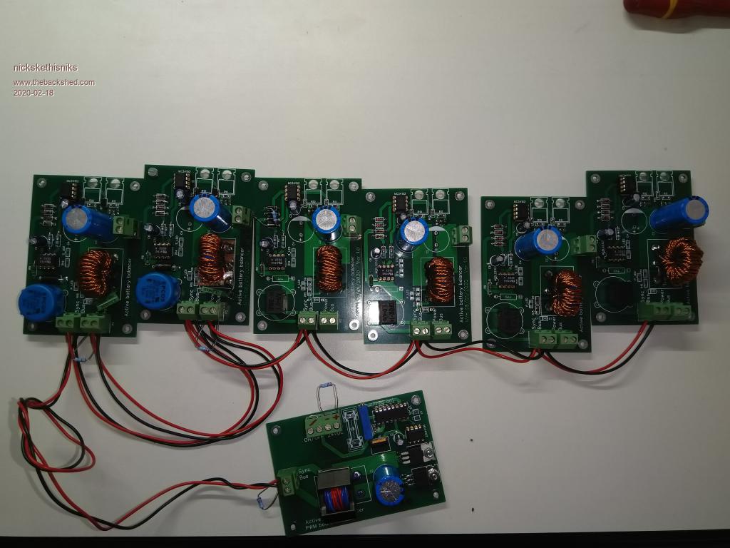
I just want to share my progress on my BMS with active battery balancer, it (could) support all battery chemistries.
Maybe a start or inspiration for other forum members.
The bms, I wanted to make something rather simple and straightforward for myself.
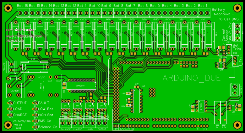
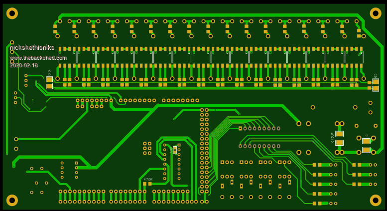
The bms itself is just a device to measure the voltages of all battery cells in a batterypack. This bms is designed for 16 cells or less, it's easy to use with less, just use another dc-dc converter for feeding the ĄC and electronics. But the concept is also working for more cells.
So the bms, the heart of the system will measure all the voltages. And will decide to activate the active balancer modules or not. It's a matter of setting the right values.
Each battery cell will have a different pcb that's connected to a central powerbus and synchronisation bus, that's the idea.
I started backwards, so the heart of the controller took to much time so that is the last part, the gerberfiles were sent, but no pcb received. So later more about the heart.
In theory the active balancer could work on it's own, but will constantly draw power so it's wise to activate the ballancer only when cells become out of ballance. That's why these modules will be controlled by the bms.
How does it work?
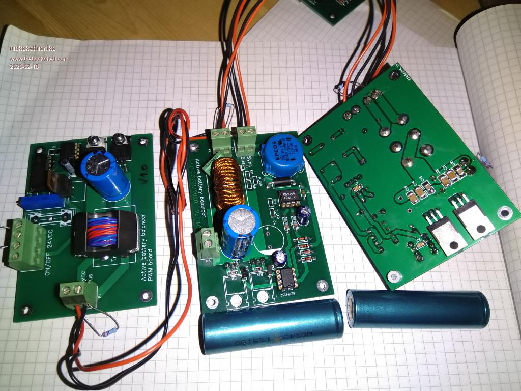
I made one board for generation of a 15V 50khz AC square wave, this signal is used for synchronisation between the balancer boards. Because all boards
need to be switching on the same moment. In my case it will also provide energy to the electronics on the balancer boards.
The 50khz is provided by a sg2525 pwm ic and goes to 2 mosfets in push pull configuration, with a hf transformer (rm10 ,n41,630)
This creates an isolated 15V 50Khz AC square wave.
On the balancer boards that ac signal is used to feed in to a "mis used" filter (ferrit toroid with 2 windings),that I use for isolation. That signal I put in an optocoupler with 2 inputs (in anti parallel) that gives me 2 outputs, 180░ out off phase. Those signals are fed in my dual mosfetdriver that drives again a push pull stage with mosfets (and act as a synchrounous rectifier).
Each board will draw about 25mA.
For the transformers on the ballancer boards I reused cores from old power supplies, I did calculatons wrong and put on to little turns, should have put on at least double. So I have a " no load " current of 50-60mA per transformer, didn't noticed it when I tested my first one. It's not realy a problem but it just consumes energy...
So ended up with more then 20 lossy transformers... Of course the higher the frequency, the lower the core loss. On the other hand they would
handle 10Amps just fine because I could use thicker wire. I could use this for LTO batteries, the lower the voltage, the lower the power loss in the core.
During testing I noticed that a higher frequency was lowering the powertransfer between the cells, could have something to do with the capacitors I used.
The average resistance of the balancer boards was +/-0.175R, that means each 0.175V difference between the cells results in balance current between the cells of 1A. I allready used IPP072N10N mosfet (100v 7.2mR) so I think lowering rdson won't help much, what can help is keep wires as short as possible, use low esr capacitors, oversized transformer...
I made an error in choosing the amount of secondary turns, the transformers are 1:2 ratio. Next version will be more like 1:10, this
will lower the conduction losses in the "powerbus" wires. And improve the power transfer even more.
Some notes:
-Although it's not needed, a snubber (rc) circuit here and there wouldn't hurt, there is some shoot thrue on the 50khz signal, an rc network damps that.
-Since mosfets don't get warm I could use fast smd mosfets with low rdson, wouldn't use that with 12V batteries, because current could be quite high.
-In fact the boards could be made a lot smaller when smd parts are used, I preffered thrue hole parts because a lot laying arround and testing the boards and the signals is easy.
-More turns are needed for lower losses in the transformer cores, plus higher step up ratio.
-Wires as short as possible, has influence on the max power transfer between the boards.
-Low esr capacitors need to be used, it has influence on the "no load" current, I used up to 4uF ceramics for one board without a lot improvement, it was the elco that made the difference.
-I noticed lower power tranfer with higher frequency with my first attempts, not tested with the latest version, it could have to do with the choice of capacitors.
-For safety, Putting fuses between board and battery wouldn't hurt, allthough this would result in higher resistance between the "magnetic coupled" cells, so
lowering the maximum possible ballance current.
Once my bms pcb is ready I'm going to put the boards in a permanent test bench circuit, to test the stability.
Pictures: I used 2 different kind of isolation transformers ( filters), the epcos filters gave the best result.
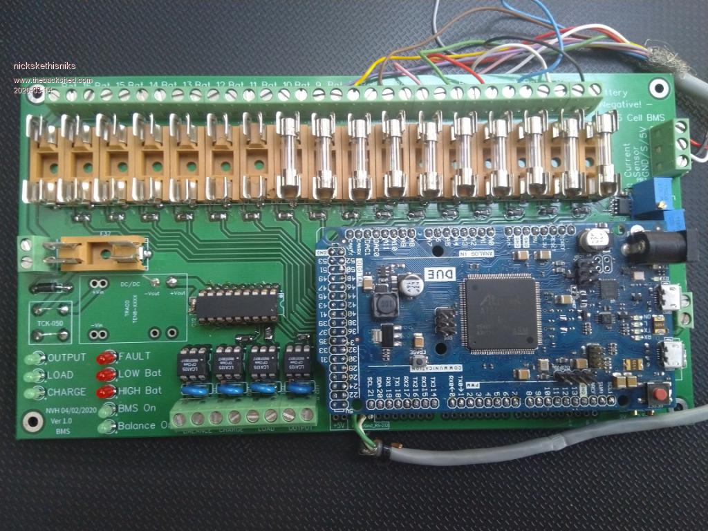
The heart of the bms, my programmer skills are limited so I choose for the arduino platform. I've choosen for the due because of the 12bit inputs, of course I could allways use a dedicated ic for it. It's compatible with arduino mega as well.
For now the board has:
-Output for load connect/disconect
-Output for charger/solar connect/disconect
-Output for active balancer
-Output for spare
-8 Leds for status
-Input for 0-5V current lem
-RS-232 for data transfer
-Input for reset button
-Input for on/of switch
I forgot inputs for temperature sensors but placed some via's for testing purpose. It's just basic at this moment, something to start with.
Edited 2020-02-18 05:59 by nickskethisniks |
nickskethisniks
Guru
Joined: 17/10/2017
Location: BelgiumPosts: 481 |
| Posted: 01:48pm 14 Mar 2020 |
Copy link to clipboard |
Print this post |
|
Update on my bms system.
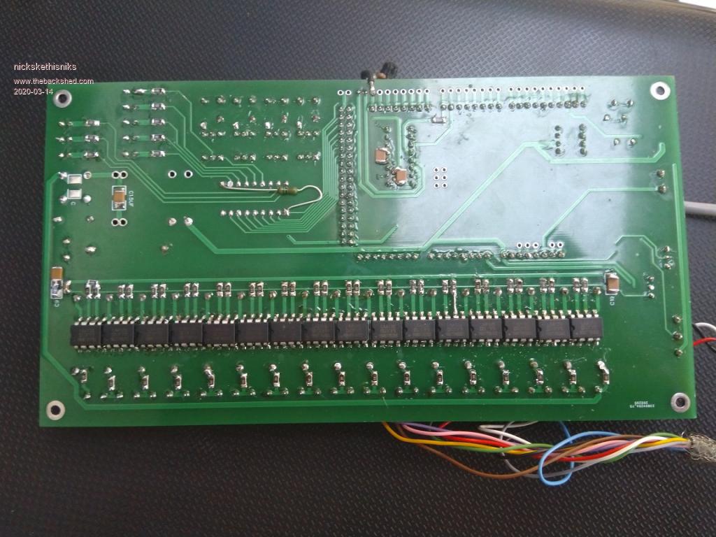
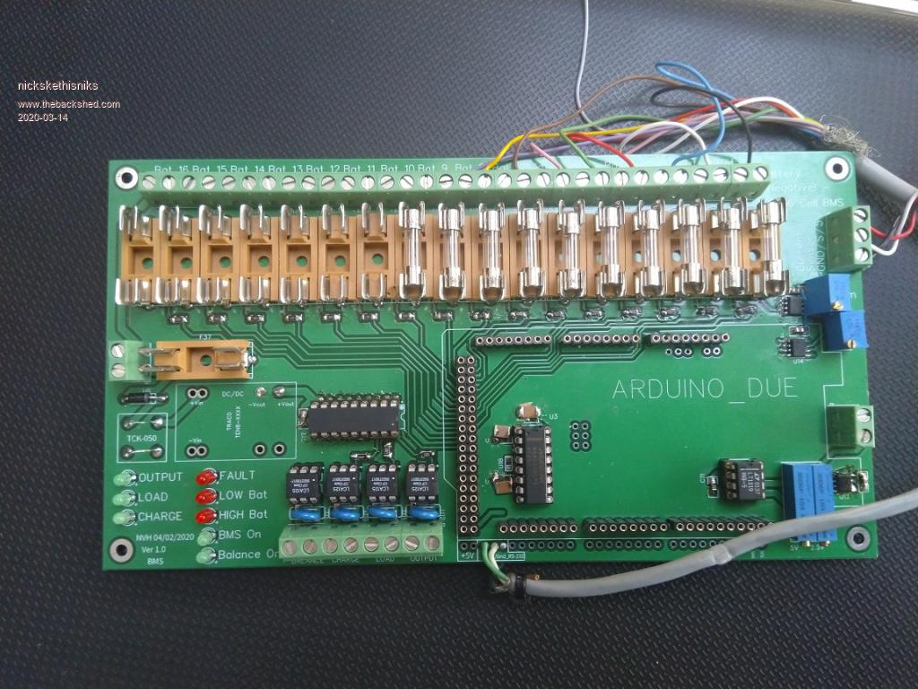
I was lucky to receive the boards of my "brain" board a few weeks ago. Since then I added parts and have tested all functions of the board.(for now I only tested a 8 cells lifepo4 pack) The arduino Mega and Due are both working with the bord, I'll keep using the DUE for it's 12bit inputs.
There were 3 mistakes,(the footprint of the 1uf capacitors around the max232 were to small, and 2 connections were just not connected with a via.) My bad, next time I will first draw the schematic. 
It looks like that I need to ad pull down resistors on my outputs of the DUE board, but could be a software bug. I still need to wait on the dc/dc converter that I will use, in the meantime I can write some code, looks like I will steal some code out of poida's nanoverter nano2 code.  The eeprom part is something usefull to adjust some parameters. The eeprom part is something usefull to adjust some parameters.
Here are some pics:
Edited 2020-03-15 04:23 by nickskethisniks |
Warpspeed
Guru
Joined: 09/08/2007
Location: AustraliaPosts: 4406 |
| Posted: 09:10pm 14 Mar 2020 |
Copy link to clipboard |
Print this post |
|
Those are really nice looking boards Nick.
You raise some interesting points about the transformers, its going to be rather difficult on the low impedance side, even with multistranded litz wire. As you correctly point out, its the dc and ac impedance there that controls the amount of power that can be transferred with very low voltage differentials between cells that we are striving for.
The way the ham radio guys go about building broadband transformers that work at tens or hundreds of Mhz is rather interesting, and we might be able to steal something from their method of construction.
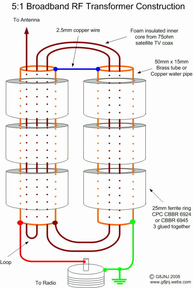
The primary consists of one turn made up of two thin wall copper (or sometimes brass) tubes, with a heavy shorting bar of the same material soldered across the far end. The thin tube takes care of skin effect, and it could be made have exceptionally low dc resistance.
The secondary consists of perhaps ten turns looped around inside the primary. The trick is then to add enough pairs of small toroids of a suitable ferrite material to the whole thing, to achieve sufficient inductance. Achieving sufficient inductance may be the biggest problem, and a higher switching frequency may help.
Its all a bit exotic, and may prove to be totally impractical for a number of reasons, but its the only suggestion I can come up with right now.
Cheers, ĀTony. |
