
|
|
Forum Index : Electronics : PCB manufacturing the easy way.
| Author | Message | ||||
| CaptainBoing Guru Joined: 07/09/2016 Location: United KingdomPosts: 1985 |
This is my process for making one-off PCBs which is now my go-to method over perfboard/stripboard and back-wiring (still do tiny bits). You will need the following software (not including your layup software, e.g. Eagle) InkScape LaserWeb Any circuits I do are always laid up in eagle anyway so making a board from there is simply a matter of clicking the schematic/board toggle on the tool bar. I lay up the board usually manually - I find this quite therapeutic. I use a laser etcher to vapourise the track borders on black acrylic painted copper-clad and as a backroom process this isn't really comfortable at track widths below 40thou (.04") I do go down to .03" to squeeze through some gaps but it is always a bit hit and miss whether a cheapie laser etcher like my Eleksmaker can actually do it accurately enough. If you have a K40 or similar they are much more accurate and I think you could take greater liberties. I try to keep tracks at .05" when I can which gives very acceptable PCBs. The process of going from Eagle to PCB has several stages but they are all quite painless and very quick. Substitute your favorite layup software as you see fit - so long as it will produce a PNG file, this process should work for you also. So in Eagle, adjust the view so it only shows the layers for bottom tracks, pad, vias and the outline: 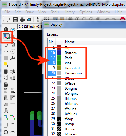 Then export the result as a PNG: 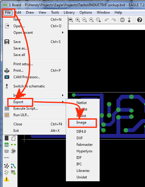 and save it out as a monochrome foil pattern. Use a minimum Dots per inch of 600 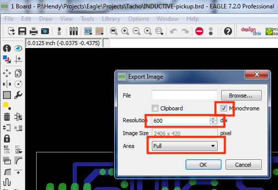 So that is the foil saved as a black and white PNG. I use InkScape to convert the PNG to an SVG vector file (which is 90% of the way to GeRBL). Open the foil PNG in Inkscape using the DPI from the file - this maintains your dimensions from Eagle: 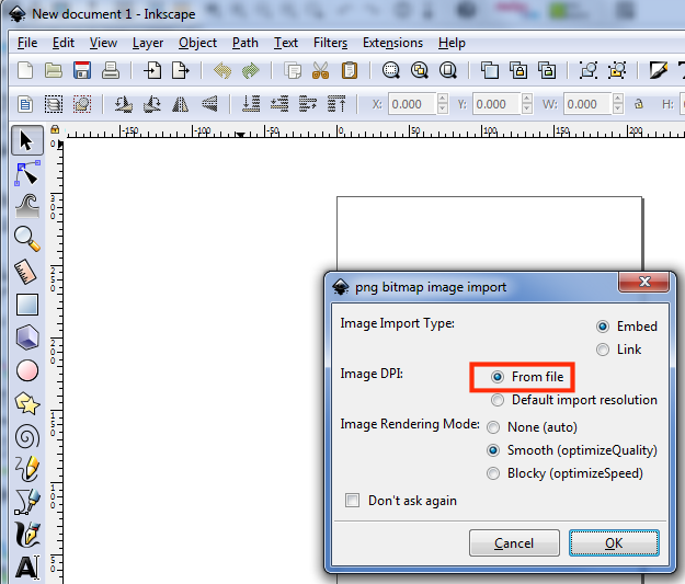 then use the path/Trace bitmap tool to trace the outline of the foil. 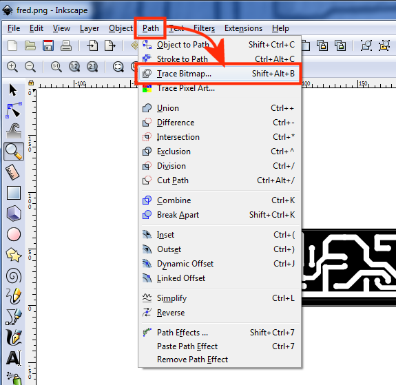 Click OK and close the tool window: 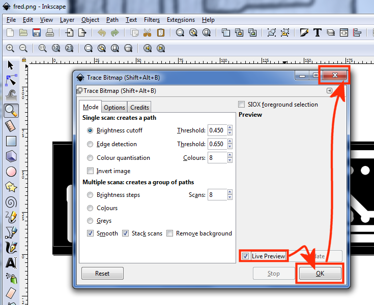 Then Save As SVG... I don't know what the difference between "InkScape SVG" and "Plain SVG" is, I always use the InkScape flavour as it comes up first and it's one less thing to change. You are know ready to etch the board using your laser. To do this I use LaserWeb. Open LaserWeb and connect to your laser 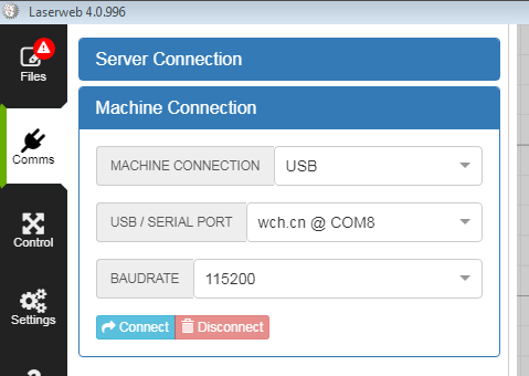 and import the SVG into the Documents control 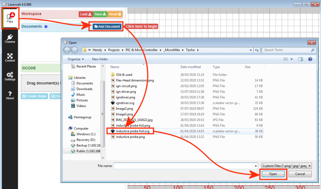 Then drag it to the GRBL generator, note the laser settings (Cut outside/100%/250mm/min) Noye also in the green box... the dimensions have been preserved from Eagle. 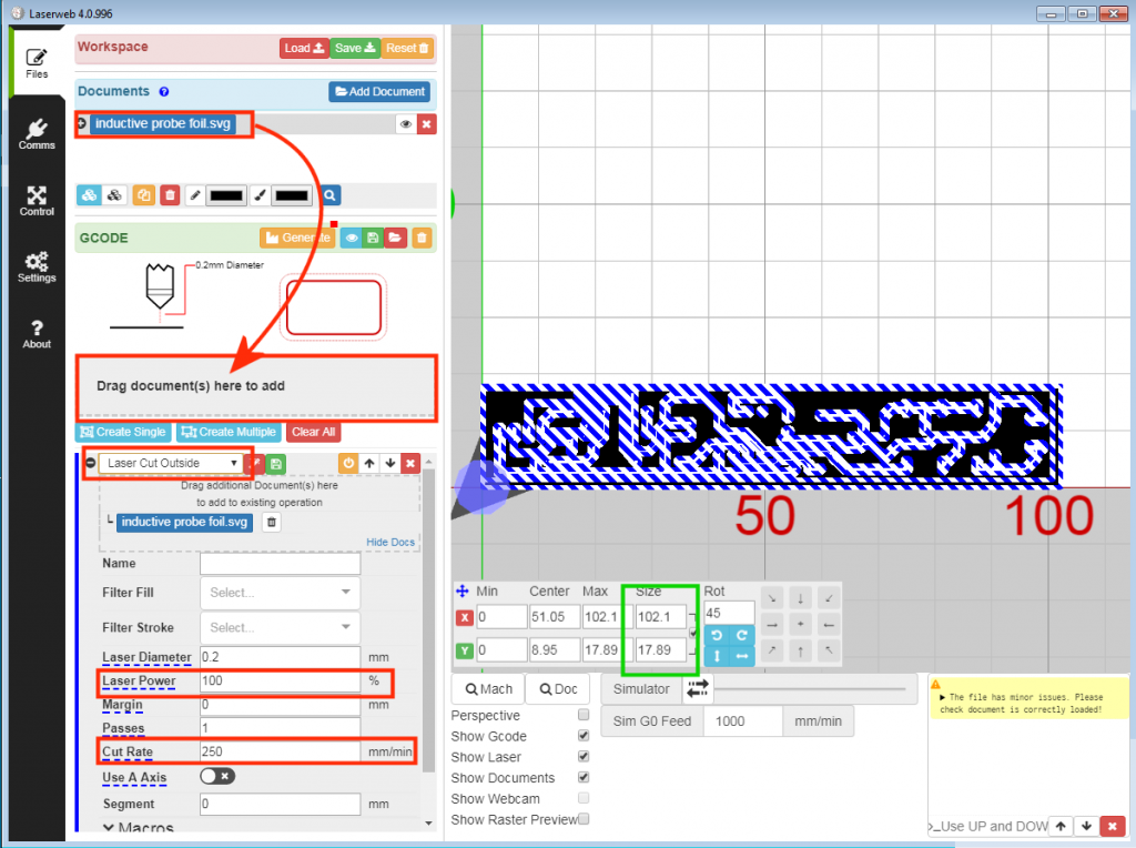 Now, my X co-ordinate is reversed which by accident provides the reversing of the foil required to get a true PCB out of the process. If your X & Y increase from south-west to north-east, you need to flip the image horizontally. Ensure the dimensions are locked then use the X-Mirror tool. set your home co-ordinate back to 0,0 afterwards as the flipping might have moved them. 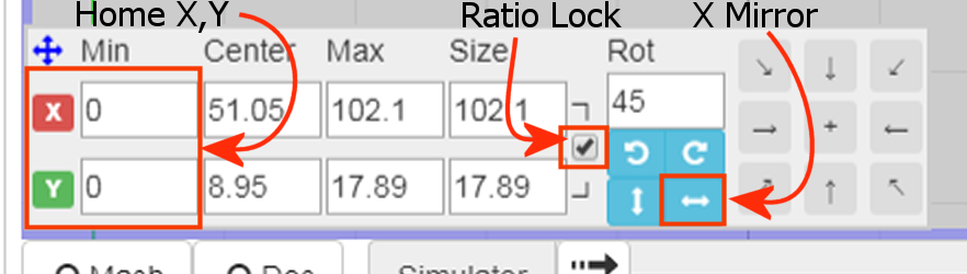 To generate the GRBL code, click the Genrate button - you may get some minor warning about the file (perhaps this is the difference between the two types of SVG?) 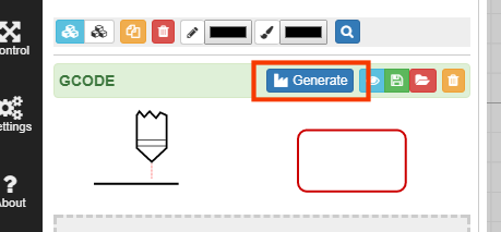 Go to the Control tab, manually position your laser head, check the dimension by turning the laser tell-tale on (top button on my laser module) to position the board as you want it. Safety goggles on, click RUN 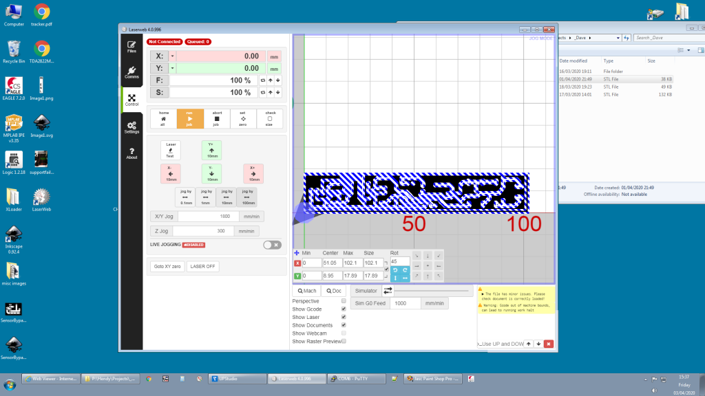 When finished, gently scrub the board under running warm water with a nail-brush and normal dish washing liquid detergent. Examine as you go that the etched tracks (actually the gaps - exposed copper) are nice and clear of particles. Etch in your favourite etchant and then clean the remaining paint off with either acetone, DCM or a stainless pot scourer (this last prepares the copper for soldering really well). Then using a DMM, check there are no shorts between the "flood" and the tracks - locate and clear any copper whiskers with a sharp point (scriber) then check all the tracks are connected to where they should with the DMM. When you are happy with the board, using the board diagram, lightly punch all the holes to be drilled - this helps centre the drill and prevents "skating". Drill the holes. Coat all over with liquid flux and assemble the board. I like to use the smallest soldering iron bit and tone out the tracks at regular intervals just to make sure I haven't bridged the etched cut but with plenty of flux it is actually quite difficult. enjoy hth h |
||||
| CaptainBoing Guru Joined: 07/09/2016 Location: United KingdomPosts: 1985 |
p.s. if your laser can't cut through the paint so well, lower the mm/min right down - Mine does a good job at 250 |
||||
| Warpspeed Guru Joined: 09/08/2007 Location: AustraliaPosts: 4406 |
Many years ago I was involved in a laser hole driller project that was intended to dill the very fine cooling holes (of micron size) in the very tough exhaust turbine blades of military jet engines. To get the laser beam down so small only required a lens. That not only reduced the spot size, it dramatically increased the energy density. Something pretty simple might enable you to do much better than forty thou tracks. Cheers, �Tony. |
||||
| CaptainBoing Guru Joined: 07/09/2016 Location: United KingdomPosts: 1985 |
Morning Tony. Thanks for the advice. Funny you should say it, I played with a lens in the beam for other things to get the beam width right down but the ones I had made the beam very conical so I had to get the focal length absolutely spot on and honestly, I am not up to it anymore... eyes are not great and looking through the safety goggles is like trying to read a newspaper with sunglasses on. The beam is about half a millimeter or so wide, so the actual thickness would appear to be OK for what I am doing - its the cheapie kit that is the problem. The carriage mechanism is just not very good for super detailed work when processing GCode (exposed belts, no linear rails). It seems better on the registration when raster etching but that gives jaggy edges on diagonals and curves. Raster etch also takes FOREVER but has the advantage that you can get a traditional looking board that only has copper flood where you put it rather than as a by-product of the way the board was produced. This was my "is it worth it" foray into laser etching and I only spent about �150-ish so you get what you pay for I guess. It has proved a point. If I invested more on the laser, something a bit better quality (like a K40 - for which I simply don't have room) then the repeat-ability of the motion is really nice and very fine tracks are possible without the variation. It is that that really makes the difference. One point with this though, once you have laser-etched the board, if you don't like the result, you simply strip the paint and try again. You aren't losing copper to find the board will be rubbish. thanks all the best h Edited 2020-04-04 17:59 by CaptainBoing |
||||
Grogster Admin Group Joined: 31/12/2012 Location: New ZealandPosts: 9044 |
EXCELLENT instructions. Lots of nice arrows etc. Nice work. Well done.  Smoke makes things work. When the smoke gets out, it stops! |
||||
| CaptainBoing Guru Joined: 07/09/2016 Location: United KingdomPosts: 1985 |
cheers Grogs - praise indeed. |
||||
| Volhout Guru Joined: 05/03/2018 Location: NetherlandsPosts: 3490 |
Hi Captain, Thanks for the very clear description. My procedure was different, I used thr CAD package to export a high resolution BMP file (or JPG), and used the Eleksmaker software to "scan" it as a picture. What I will play with is the opposite of warpspeeds suggestion: De-focus the laser a bit and bring the travel speed down. That way it wil carve slightly wider channels through my black paint, and may result in wider gaps (fewer shorts after etching, or while soldering). I will checkout the "laserweb" software. That seems a nice piece of code. Volhout By the way, did you ever update the firmware on the Eleksmaker ? There apparently is a newer firmware that is more accurate, and has laser power adjustment(PWM) when the traction motors slow down for a corner. I tried that new code (I recall it is version 1.12 or so), and it improved, but was incompatible with the Eleksmaker Windows software (that software checks for version 0.95, and refuses to work otherwise). I manually edited the 1.12 firmware to give out version 0.95. And manually edited some of the parameters. I also saw in a Youtube video that there are better stepper motor driver, that have improved microstepping. It could improve (if you have mechanically tuned all play out of the system). PicomiteVGA PETSCII ROBOTS |
||||
| CaptainBoing Guru Joined: 07/09/2016 Location: United KingdomPosts: 1985 |
Hey Volhout. yes that might be your problem - you have the laser pin-sharp and my old man eyes didn't get to that and it counts as a happy accident again. LaserWeb is a nice piece of software... As with a lot of Open source, it seems flaky at times and I have had mystery blue-screens at random which are either LW or the driver for the laser... but the driver is a standard CH340 which I use loads of other places without issue. I did an experiment where I left the machine on after lasing which left the driver loaded but quit LW... no blue screen so I am pretty sure where the problem lies. The code on the bsod seems to be all sorts as well... rather than one consistently. So beware. here is a pic from my microscope of an etched copper board with a steel rule across it for measurement... it actually is probably 0.1 - 0.2mm ish in reality. 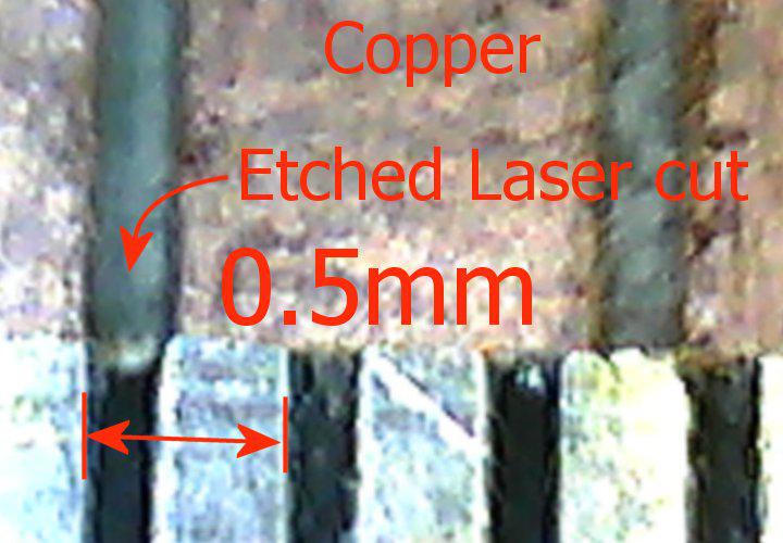 I did upgrade the firmware on the Eleksmaker. Its controller is simply an arduino but that makes it easy coz of the boot loader. Can't remember the name of the utility I used (I am in the office and that is on the workshop PC) but I will post back later with the GRBL version as well. Over-cutting on corners is a problem when I am engraving (but not etching a pcb) and I have noticed burning when doing wood. A friend locally makes violin cases and I produce a rather nice little wooden maker's plaque for him, I had to resort to raster scanning (and set the beam width down to a false 0.1mm to get rid of stripes) to avoid burnt corners. That new firmware may well be worth investigating. Cheers for the heads-up. Edited 2020-04-07 01:38 by CaptainBoing |
||||
| Volhout Guru Joined: 05/03/2018 Location: NetherlandsPosts: 3490 |
Hi Captainboing, Yesterday looked for the latest GRBL code. For the eleksmaker software, grbl version 0.9i is needed. The latests grbl on github is grbl 1.1h. I tried compiling that, but it failed on my linux machine (running out of memory on the ATMEGA328). Then I tried compiling on a windows machine, and the program fits in memory, with 200 bytes free of 32k. I did not know there was a difference in compiler efficiency between arduino linux and arduino windows. Both use AVR-GCC if I remember right. Anyway, compiling works. Now I have to get the defaults (the $$ settings) right, and the version string set to 0.9i... Volhout PicomiteVGA PETSCII ROBOTS |
||||
| Volhout Guru Joined: 05/03/2018 Location: NetherlandsPosts: 3490 |
Hi Captainboing, I just watched a video from Marco Reps on YT on all the improvements he made to the Eleksmaker. But even after all the improvements, when I saw the result shown in his video, it had the same artefacts that I observed. I am not sure this is in the EleksLaser hardware, in the Arduino nano grbl code, a setting, or in the code that controls the machine. Could be any of those. 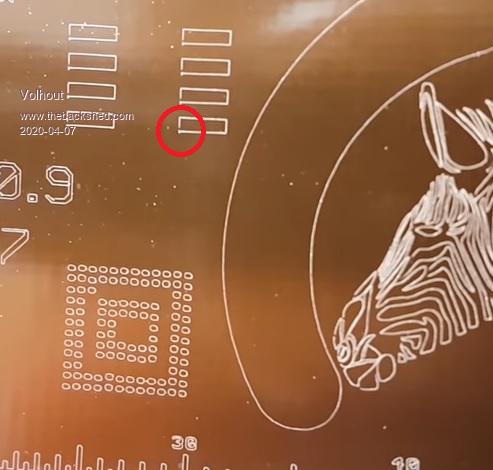 Volhout PicomiteVGA PETSCII ROBOTS |
||||
| CaptainBoing Guru Joined: 07/09/2016 Location: United KingdomPosts: 1985 |
I can grab the settings off mine if that helps to get you started? Was not aware the compile would be any different either but I am very much a user for things Arduino so I downloaded the latest compiled version (actually think I am on "e"). Yes Marco is an inspiration and his Eleksmaker vids are what led me down this route. I am convinced the Eleksmaker is really a toy, good enough for most things and cutting bits of wood with humourous jokes but for serious stuff the mechanism is just too basic and without linear actuators there will simply be too much slop for serious application. There are better machines about and the K40 seems to be one of those within my budget but I simply don't have the room for it... it would have to sit on some bench and i have precious little of that available as it is. For now, knowing the Eleksmaker's limitations, I can work around them... I only use it for the odd PCB, so if production were involved I would always get them made (in my case) by JLC... prices for 10 off excellent quality boards just isn't worth doing a crappy job myself. h Edited 2020-04-07 18:09 by CaptainBoing |
||||
| Volhout Guru Joined: 05/03/2018 Location: NetherlandsPosts: 3490 |
Hi Captain, I it correct that there is no visual feedback where the cutting progress is in the screen? Volhout PicomiteVGA PETSCII ROBOTS |
||||
| CaptainBoing Guru Joined: 07/09/2016 Location: United KingdomPosts: 1985 |
errm... can't say i had noticed, I am always either watching the laser cut or vacate the workshop (no fume extraction, laser is by the door) There is a logging window bottom right, perhaps it lists the gcode there as executed? |
||||
Revlac Guru Joined: 31/12/2016 Location: AustraliaPosts: 961 |
@CaptainBoing Thought I would try this method for one off boards. Question: what settings did you find best for Trace bitmap.....Never mind, I see the settings are somewhat different in this version of inkscape. After some time spent mucking around with settings and many mistakes (still learning the program) I have found good results with single scan, speckles, smooth corners and optimise left unchecked. And I didn't use Simplify, It might be ok for some, it gives a lot of rounded edges and curves but if necessary we can move the nodes to fix it up or widen the tracks. Its also good to remove the underlying image that's hiding under the traced image...didn't see it there the first few times.  Going to try this with a K40 shortly. Plenty of power...  Cheers Aaron Off The Grid |
||||
| CaptainBoing Guru Joined: 07/09/2016 Location: United KingdomPosts: 1985 |
Morning Revlac I used the defaults tbh, they worked without any tweaks for me so I just left them. I would love to see the results of this on your K40 - I letch after one as I think it's motion being way more professional - especially the static laser with right-angle mirror guiding. Should be way superior. One thing i would really like to crack is the 40thou thing, but then I would have much tinier cuts and more chance of bridging when soldering. I do use the above method a lot for small runs and small boards, I had to butcher a production board (because of a silly mistake I made) and a tiddly 3-channel level-shifter was produced in under an hour which was "dead-bugged" onto the board and fixed things. Far from ideal but also not a re-order and 12 day delay. I make loads of little add-ons like this. the level-shifter, a soft power-off conversion board etc. and the eleksmaker is most at home doing small tasks like this. I did etch a one-off 6"x 4" as a raster (so no "incidental" copper flood) - it did a reasonable job but took over 11 hours with the beam set to 0.075mm to avoid the "jaggies" (with mixed success). But the board turn out ok and is in use. Saves me having to backwire or use stripboard. can't wait to see your results - good luck and have fun p.s. when cutting with LW, there is a count top left of the number of movements remaining, so there is a progress/countdown of sorts. |
||||
| Swartz Newbie Joined: 15/12/2020 Location: United StatesPosts: 18 |
maybe I missed it , but so you have any specs (Watts , wavelength , etc.) for the laser you use in this application? Thanks! Edited 2021-07-10 15:22 by Swartz |
||||
| CaptainBoing Guru Joined: 07/09/2016 Location: United KingdomPosts: 1985 |
it's a blue LED laser, I think 5W. will correct later if i am wrong Edited 2021-07-11 16:35 by CaptainBoing |
||||
