
|
|
Forum Index : Electronics : GridMaker: A 10KW 3-Phase inverter build
| Page 1 of 2 |
|||||
| Author | Message | ||||
Haxby Guru Joined: 07/07/2008 Location: AustraliaPosts: 426 |
This is the build thread of my 3-Phase 10KW inverter. CodeName: GridMaker After building the single phase version, and with the generous help of Warpspeed, and Poida's software skills, and realising that I have 90% of the components to build a 3 phase version, I couldn't get the thought of building one out of my mind. The inverter will use mostly recycled aerosharp solar inverter parts. Capacitors, transformers, current sensors, etc. Unlike the first build, due to the sheer amount of components required, I will be using lower quality (possibly counterfeit) parts for the IGBT's and mosfet driver ICs. I'll have to check all parts before turning on! But with each IGBT being powered by a separate supply, I don't expect too much smoke.  Power will come from a completely unmodified Nissan Leaf battery, using the built in Nissan battery management system (BMS). The battery pack has the BMS and contactors and current sensors, and earth leakage sensors built in, so why reinvent the wheel? It's a lot safer than building my own. To control these features, a gentleman known as "Wolf" from Wolftronix has built a relatively inexpensive CAN bus controller. It's a little black box that plugs into the data socket of the battery pack. The controller controls the contactors, precharge relay, and can be programmed with many safety parameters such as over current, under voltage, over voltage, temperature, etc. Importantly for us, there is a programmable relay output that can be used to end charging the pack. He calls it a pack sniffer but it's more a controller. Details here. Have a look at the "modify config files" video to see what it can do. (It's a lot!) The Nissan Leaf battery uses 96 series connected lithium cells, and has a nominal voltage of approx 360V. This is identical to the Tesla Model 3 full pack. Now I see a Model 3 on the road almost every day, and that's great news for us because inevitably, some will get written off.... The model 3 packs are basically impossible to disassemble out of the heavily-glued-together module configuration, so there isn't much demand for them in the salvage market. That's more good news for us, because the prices of these very-very high quality bullet proof packs will reflect the demand. Someone just has to reverse engineer the communications for them, and I'm sure plenty are working on this right as we speak. Anyway, I digress. Some pics of my progress. I'm building 3 of my single phase power boards, one for each phase. This time I'm using GW80V60DF IGBT's. They are rated at 120A at 25 degrees C, so they should withstand a short across the output for the duration that a C-Curve breaker can trip. This is a really important factor, and makes designing for over-current situations pretty simple. The heatsinks will need to dissipate 40W each at full load, so a fan will be required for each one. The 4 IGBT's on the far center only need to dissipate 1W at 50% duty cycle at most, so I won't put them on a heatsink for now and see how hot they get. 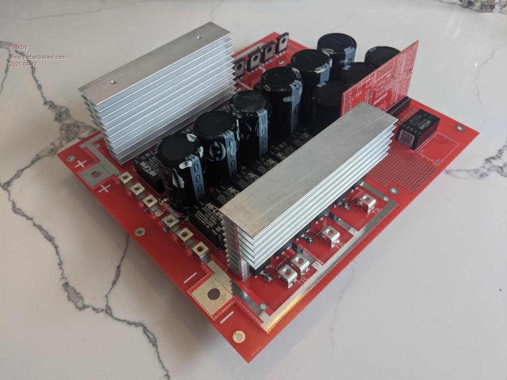 And here is the control board running Poida's code. I like through hole components as much as the next guy, but this has to run a total of 48 IGBT drivers, so the component count is very high. If I didn't use SMD components, it would have to have been a large 4 layer logic board. Not very desirable. So I went with a Mega 2560 MINI, and squeezed everything on one riser board that could live on the middle power board. It's no higher than the heatsinks, so the whole single board can still fit in a 2U rack mount box. You can see the 16 pin IDC connectors that go to each power board. The 2 pin connector is the on/off control, and the 4 pin connector is voltage feedback from 3x off-board transformers. I'll coat it heavily with some conformal coating spray once all the bugs are ironed out. 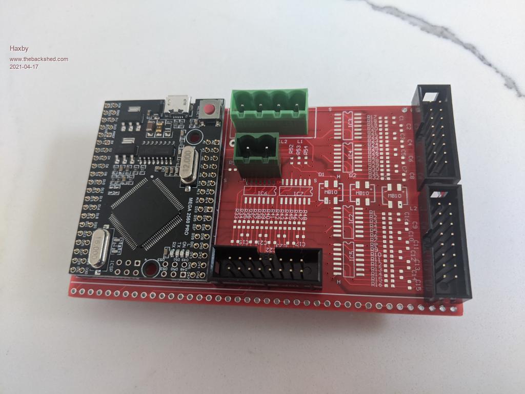 I haven't tested the board yet, just waiting on components, I only scoped the mega mini to see the familiar step traces. Hopefully I haven't stuffed it up! |
||||
| rogerdw Guru Joined: 22/10/2019 Location: AustraliaPosts: 955 |
Congratulations Phil, a very gutsy build. Wishing you all the best with it. Seeing your workmanship so far I'd love to see you tackle toroids as well. I reckon you'll find them much easier than you think. Either way, if you can make it work with existing toroids that's awesome. Cheers, Roger |
||||
| poida Guru Joined: 02/02/2017 Location: AustraliaPosts: 1480 |
This is outstanding. wronger than a phone book full of wrong phone numbers |
||||
| InPhase Senior Member Joined: 15/12/2020 Location: United StatesPosts: 178 |
He's a man outstanding in his field...  |
||||
| Warpspeed Guru Joined: 09/08/2007 Location: AustraliaPosts: 4406 |
Certainly EPIC. Cheers, ĀTony. |
||||
| nickskethisniks Guru Joined: 17/10/2017 Location: BelgiumPosts: 481 |
Nice project, I will certainly keep an eye on it. I like the compactness but maybe you want to make your control board bigger to include some features: - some communication buses - maybe some pre-charge outputs - output for output relais - a few status LEDs - dedicated power supply - lcd ... Mmm, you can also do that externally.  |
||||
| Warpspeed Guru Joined: 09/08/2007 Location: AustraliaPosts: 4406 |
External would be better for several reasons. More customised functions would be nice, but the big obstacle would be sufficient I/O ports to do it. Three Warpverters require the constant full time use of three eight bit parallel ports. At least a fourth port would be required for extra sensors and outputs needed for bells and whistles type extra features. Not only that, the risk of making software additions and changes to add extra features carries some slight risk of crashing the main inverter software, which could be catastrophic. Much safer to generate some very robust and well proven core Warpverter code, and not mess with it. I did it all with just very simple crude easy to understand hardware. A Nano or something similar with a few sensors, and a display, plus some relays, and it could do just about anything you could ever wish for with some very simple non critical code. Cheers, ĀTony. |
||||
| Haxby Guru Joined: 07/07/2008 Location: AustraliaPosts: 426 |
In my single phase high DC voltage warpverter I have found EMI to be surprisingly intrusive into the processor that I was using to control the precharge relay. I can now see why there is a common mode choke and ferrite clip everywhere you look on the aerosharp boards. It's not just for EMC compliance. So if I use another board to control auxiliary functions it will need a careful approach to EMI. I definitely prefer to leave the mega doing one job only. No long leads coming out of the processor with the exception of the logic signals going to the other power boards (which I already feel uncomfortable about). In my case the wolftronix controller controls the DC input over/under voltage, as well as the precharge relay built into the Nissan leaf pack. So let's see what else is required.... 1 overcurrent protection for the output 2 contactor to energise the output once the inverter has soft started the 3 phases, and to de-energise before power off. 3 heatsink fan temp monitoring & control 4 readout of voltage, current and watts delivered. Except for point 2 above, there are DIN rail solutions to all of the above...so maybe that's the best way to go. One thing that Poida could consider implementing into the code is a test to see if voltage feedback is actually connected at all on startup. A feature that the EGS boards have is that they shut down if they don't sense a feedback voltage within a second of powering up. This is a good feature because if the feedback voltage is disconnected, the output can go to 400v+ and stay that way till all transformers saturate and/or all appliances blow up and/or all IGBTs go kaboom! |
||||
| Warpspeed Guru Joined: 09/08/2007 Location: AustraliaPosts: 4406 |
Quite right Phil. EMI was a very major consideration in the design of the original Warpverter. The only direct connections to the control board are battery and ground. Any noise spikes on the battery feed are effectively removed by the dual slope integrator in the analog to digital voltmeter. It very effectively removes noise without slowing down or corrupting the readings. All the gate driver circuits are balanced and fully optically isolated, pretty much ensuring nothing can get back onto the driver board that way, or into the gate drive signals. There is no voltage feedback in my design, which eliminates a great many possible failure modes. Any powerful inverter is going to generate some EMI, its just not possible to switch tens of amps very quickly without inducing some very nasty voltage and current transients into other parts of the system. Its a further reason I decided not to run a microcontroller in the final design. All of my earlier prototype designs did use a microcontroller of one type or another, and I used that same software to program all 256 lookup tables into a huge EEPROM. Hardware may occasionally glitch but it cannot totally crash and burn in the same way software can. As soon as you start bringing great bundles of wires to and from various other parts of the system back to the main control board, it potentially opens up a lot of nightmare EMI possibilities. Its possible to do of course, but its not going to be simple or easy to diagnose intermittent "manifestations" or occasional odd misbehavior. Best to keep the whole system as simple and bullet proof as possible. Any extra features can be added on later as a separate entity, and quarantined from the main inverter drive system. Cheers, ĀTony. |
||||
| Haxby Guru Joined: 07/07/2008 Location: AustraliaPosts: 426 |
Warp you've got me thinking whether I should have buffered the nano output with another hex inverter gate before breaking out the signal to the big bad world: Top pic shows what I did. Bottom pic shows what might work better. Thoughts appreciated! (As always) 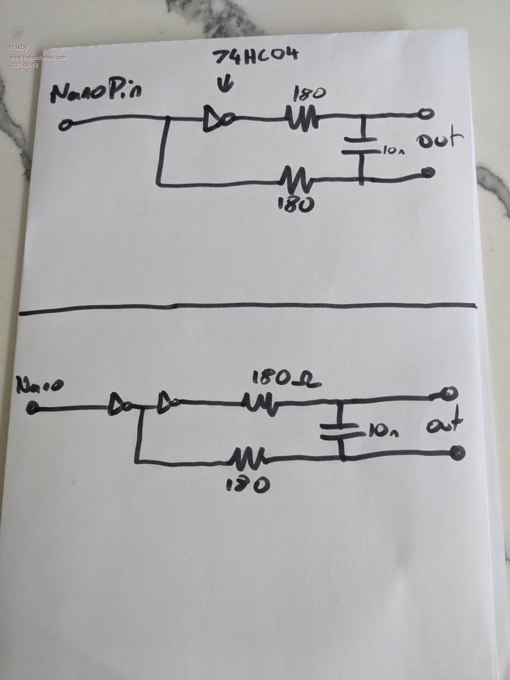 |
||||
| Haxby Guru Joined: 07/07/2008 Location: AustraliaPosts: 426 |
Gents, I'm considering scrapping the logic board and re-designing a new board for better EMI protection. As it is now, there are 24 wires coming out of the processor that are going straight to each power board (via 180 ohm resistor). The distance is about 30cm. I'm thinking of optocoupling each one before it exits the board. I'm concerned about common mode noise being picked up. Am I paranoid? |
||||
| poida Guru Joined: 02/02/2017 Location: AustraliaPosts: 1480 |
I think you could use optos for the output of the board, and have optos also on each inverter board. It seems like a lot of bother but I see it as differential pairs for all signals. This adds up to 48 wires, 24 pairs. 24 optos on the controller, and 24 on the inverters, 8 per phase. This will isolate a lot of rubbish from the logic source. I expect there are quad optos on SOT format, maybe even 8 optos per package. I have not bothered to have a quick look in digikey. (looks at first thing on digikey...) TLP292-4 is only $0.67 AU with 4 channels. So you need 6. All 24 opto outputs could be driven by a single DC source, isolated from all the rest of the logic. Ahh, but then the 24 outputs will not be isolated from each other. Maybe no problem then, since we need about 5-10mA to drive an opto diode and EMI is usually of the order of a few uA. wronger than a phone book full of wrong phone numbers |
||||
| Haxby Guru Joined: 07/07/2008 Location: AustraliaPosts: 426 |
My (possibly unfounded) paranoia is that EMI could get back to the mega processor and lock it up. So I'm contemplating either running each mega output through a hex inverter 74hc04 for "some" protection or completely isolating each output with an optocoupler. I don't have any experience with EMI so I don't know how valid my concerns are. But a locked up processor would be game over to 48 IGBTs! To be clear, the signal wires are already "balanced" in that each pair already connects to the LED of the igbt driver chip. Nothing else. No ground loops. But even though there are no ground loops, I think that having 24 pins of the mega, coming out 30cm from the board, completely un-buffered, may be a bad idea. How bad an idea is hard to judge for me. Could just having a ferrite clip-on bead be enough? Not sure. |
||||
| Warpspeed Guru Joined: 09/08/2007 Location: AustraliaPosts: 4406 |
I believe you definitely need opto isolators located right at the mosfet gates to prevent anything upsetting the gate drives directly. Its right at the individual switching bridges that all the electrical violence is at its worst. I believe we are already all in full agreement that the lower mosfet gate driver circuits in the bridge require full galvanic isolation, and the same treatment as the upper mosfet gate drivers. The driver should bond as closely as possible directly to the mosfet source to work independent of the very noisy main system ground. At the other end, the control board is just driving into a fully floating LED through a rather long twisted pair. Almost nothing external can get into that to upset the gate drive signal. Any induced common mode voltage will be shunted by the low impedance of the buffers and the 180 ohm series drive resistors. I cannot see that ever being a serious problem, especially if the heatsinks are all grounded. "Live" heatsinks connected directly to the lower mosfet drains may capacitively couple into the gate driver leads, but if you are aware of this possibility, its not difficult to physically separate the drive wires from any live heatsinks. Unless the drive wires actually lay directly over a live heatsink for quite a distance, I doubt you will have any issues. The real evil is in the overall system grounding. Nowhere will there be a nice solid noise free ground that all your analog and digital systems can be referenced to. This becomes especially bad as there are four inverters not one. Phil will have twelve inverters running, and as long as the whole thing is thought right through, there should not be any more noise or EMI problems than with just a single inverter. Cheers, ĀTony. |
||||
| Warpspeed Guru Joined: 09/08/2007 Location: AustraliaPosts: 4406 |
One further thought... If capacitive coupling into the long gate driver leads does prove to be a problem, you could always use twin screened (microphone) cable. Do not connect the screen to the microprocessor ground, but connect just one end only of the screen to the main dc power system ground at one end or the other. I cannot see this being necessary, but its always good to have one extra trick up your sleeve. Cheers, ĀTony. |
||||
| wiseguy Guru Joined: 21/06/2018 Location: AustraliaPosts: 1297 |
A bit of paranoia is actually healthy in applications like this. In my opinion & experience, in noisy environments I place a minimum ~100 ohms in series and close to each output from the micro. Looking back towards the uC any outside noise has a low pass filter of 100Ohms and a few pF which greatly attenuates the fast edges that are likely to be the cause of any trouble. Using an opto for each output I think is overkill. I like your proposed scheme of 2 x HC04's and the 2 x 180 Ohm resistors, but I would still include a series resistor between the uC and the first HC04 buffer if there is room, nothing wrong with belts and braces. As Tony suggests, keep the Opto drivers as close to the FETs/IGBTs as you can manage is also optimal. Probably obvious, but good PCB layout then to keep external (noisy) traces at the edge of the board & well away from any of the uC pins & traces. If there needs to be a physical connection/s between the uC PCB ground and the power stage ground (ie for measuring Vin etc) a ferrite bead/s can also help. "having 24 pins of the mega, coming out 30cm from the board, completely un-buffered, may be a bad idea in my experience" Totally Agree. If at first you dont succeed, I suggest you avoid sky diving.... Cheers Mike |
||||
| Murphy's friend Guru Joined: 04/10/2019 Location: AustraliaPosts: 678 |
Interesting topic about grounding. The heatsinks (not 'life') of my warpverter are floating, so you suggest I connect them to the negative battery rail? My warpverter is still waiting for a corrected PCB to arrive but I'm happy to remedy any possible other problem before I fire it up again. |
||||
| Warpspeed Guru Joined: 09/08/2007 Location: AustraliaPosts: 4406 |
If they are truly floating, it certainly would not hurt to ground them. Cheers, ĀTony. |
||||
| Haxby Guru Joined: 07/07/2008 Location: AustraliaPosts: 426 |
To completely isolate the mega mini processor from the power electronics, I'm considering signalling each IGBT through fiber optic cable. I'm thinking of using common Hi-Fi audio industry fiber optic cables known as Toslink cables. They appear to be just an LED for the transmitter and a transistor for the receiver... So just a very long optocoupler: 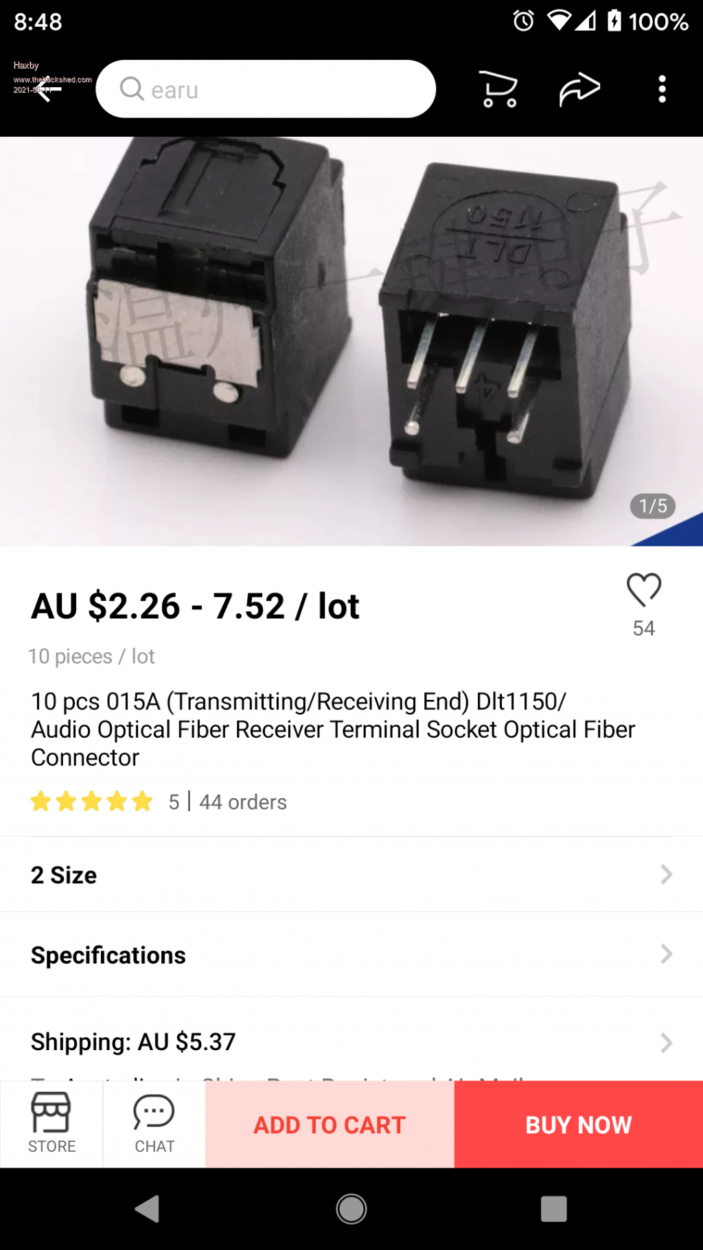 This would put my mind at ease once and for all with regard to capacitive and EMI issues. Any thoughts on this? Not sure if I should have one optical cable per igbt or one optical cable per 2 igbts (half bridge). One per igbt would require 16 optical cables per phase, so 48 optic cables total coming from the processor!!! If I used 1 optic cable per half bridge, I'd "only" need 24 total but then would have to add a dead time circuit at the igbt end, which would add complexity.... Decisions decisions.... Anyone here used audio based optic cables for something like this before? The other more professional and expensive types are the HFBR-0500 by Avago, but I'd imagine the cheap Ali express ones would be fine. |
||||
| Warpspeed Guru Joined: 09/08/2007 Location: AustraliaPosts: 4406 |
I think personally its probably overkill, but no harm in doing it. If the whole EMI concept is thought right through, and there is a definite plan regarding layout and grounding, most of the potential problems will never arise in the first place. There is a lot more to all this than just getting a schematic from somewhere and connecting up all the parts to each other. Cheers, ĀTony. |
||||
| Page 1 of 2 |
|||||
| The Back Shed's forum code is written, and hosted, in Australia. | © JAQ Software 2026 |
