
|
|
Forum Index : Electronics : My Power Jack HF 1200W DC12V/AC230V inverter
| Author | Message | ||||
| hary Regular Member Joined: 15/04/2019 Location: FrancePosts: 89 |
Hi I received the 4 new IGBT for the 2nd stage of my broken Power Jack HF 1200W DC12V/AC230V inverter.(the 2 on the right were blown up) I replaced them all, but before putting all the power on them I'd like to be sure everything is ok. 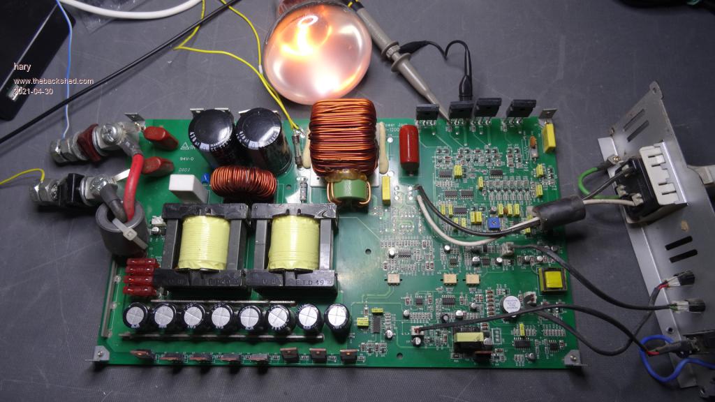 So I put a light bulb in series with the DC250V fuse on the line before the IGBT.  And I check the gate signal on one of the IGBT :  I put my unique differential probe on the AC220V output. Here is the 2 ugly oscillogram I get (yellow is the gate signal at about 21kHz, blue is the "50Hz sine wave": 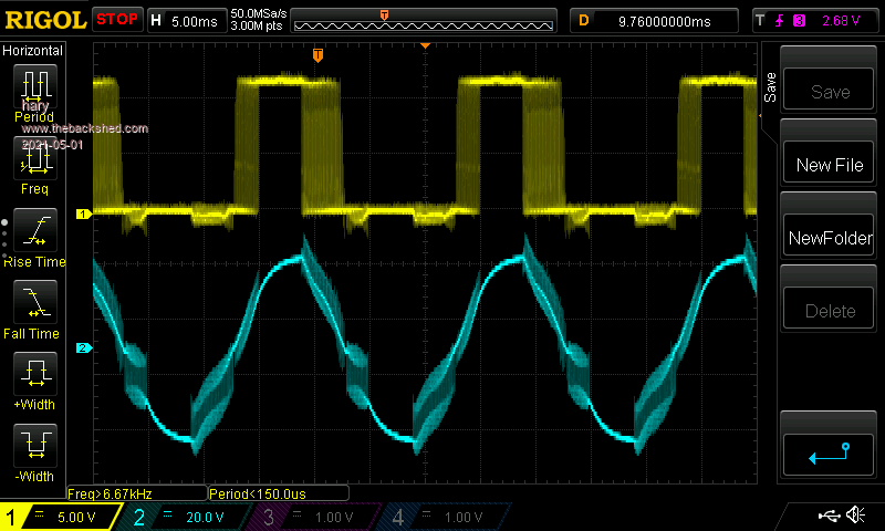 Plus the 2 IGBTs on the left stay cool, the 2 on the right get pretty warm with no load. Plus the light bulb stays on even after the start-up ? Is that normal or should I suspect something wrong ? I don't know where to go next ? Any advices appreciated. |
||||
| noneyabussiness Guru Joined: 31/07/2017 Location: AustraliaPosts: 506 |
Definitely not normal, no load should be virtually zero... I would change those surface mount npn/pnp totem pole drive transistors... then back track from there.. judging by the " 339 " comparators it has a similar setup to the low frequency PJ's, so would check them too.. I think it works !! |
||||
| hary Regular Member Joined: 15/04/2019 Location: FrancePosts: 89 |
I been trying to figure out what is going wrong. My assumptions are : As the light bulb in series with the 360VDC fuse stays on with no load on the AC230V output, it's still taking some power and that power has to be dissipated somewhere. The only parts the power can be dissipated in are the 2 right mosfets which are warming up after a while. (good I put that light bulb to protect from any shorts). If I look at a full H-bridge :  It seems as Q3 and Q4 are conducting at the same time creating a short between DC360V. As the light bulb only lights up slightly, Q3 and Q4 are not conducting together 100% of the time, the average voltage at the bulb isn't DC360V. Then I put the scope at Q3 and here is what I get yellow trace: 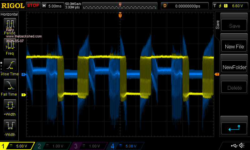 As you can see, it's larger than 50% duty cycle. I thus think it was obvious that Q3 was overlapping Q4 duty cycle time, and the explanation was clear. Q4 on the other hand seemed to look ok with less than 50% duty cycle On time : 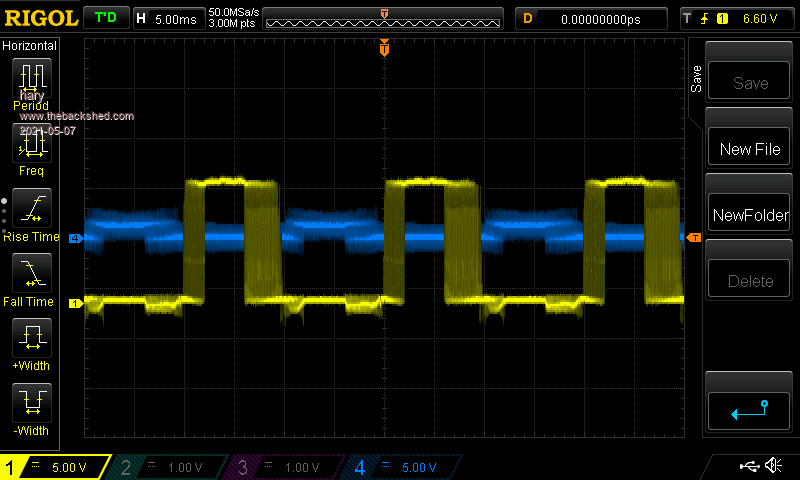 I then checked Q1 and Q2, and unexpectedly, Q1 showed more than 50% duty cycle On ! Q2 seem under 50% duty cycle On. So both of the High side mosfets seem to have more than 50% duty cycle On. But then why Q1 and Q2 are not warming up as Q3 and Q4 do ? I don't have isolated input on my scope, only a cheap homemade deferential probe that gives the strange blue trace at 20kHz spwm frequency. So I can't get proper trace for each mosfet at the same time. Am I digging in the right direction or am I completely wrong ? Is there not a way to diagnose the problem before blindly replace parts ? Edited 2021-05-07 06:07 by hary |
||||
| wiseguy Guru Joined: 21/06/2018 Location: AustraliaPosts: 993 |
Maybe you can remove VBus from the top of the H bridge and get a much better look at the 4 different gate drives safely with less pollution from whatever fault may exist. It would be preferable to stop the Dc/Dc from generating the VBus but you may have to fool the microcontroller that VBus is ok or it might inhibit drive. That might be the function of the single white opto closest to the transformers. I like your input wire size safely bolted up ! If at first you dont succeed, I suggest you avoid sky diving.... Cheers Mike |
||||
| hary Regular Member Joined: 15/04/2019 Location: FrancePosts: 89 |
Thanks wiseguy for giving me some direction. Yes, you're right, there is no spwm driver signal without some at least DC200V on the VBus. You're probably right about that white opto. But I guess, I cannot just remove the series light bulb to open the DC360V circuit open ? Overwise, the first stage might go up to a very super high voltage with its feedback fooled. I guess, I need deactivate its drive by any trick ? In fact, that might not be a so big problem as it has this fuse (same place I put the series protection light bulb). In case the fuse blow up, that opto wouldn't have feedback? Or maybe the feedback is before the fuse ? I have to check that . . . I'll come back after I get this information. |
||||
Revlac Guru Joined: 31/12/2016 Location: AustraliaPosts: 961 |
I know a little about the Voltronic type inverter, Some of this might be relevant and some likely not. The gate drive on the Voltronic use's ACPL-T350 opto's to drive the 4 STGW80H65DFB IGBT's, output through the usual choke then capacitor and then the EMI filter, output relays etc. To my knowledge The gate drive will not run until the VBus reaches its working voltage, around 400-420vdc last I checked, this can (vary rare) go over voltage if something like a heatgun (with half rectified speed control) is used and is the only load on the Inverter, the over voltage is detected, the output relay opens and I the think the gate drive also shuts off until the error clears (5 seconds or so) and starts up again. The voltage from the transformer and before the diode rectifier stage (I believe) has its own feedback loop, likely back to the SG3524, and this section will continue to run, unless something else happens, smoke or something drastic. So the voltage regulation before the bus and after is 2 separate parts, as I understand it. Don't know if any of this is much help, but some of it works in similar way to your inverter, don't know much else about it. Trying to trick the HV gate drive to run could be difficult but someone smarter than me could perhaps get it to work. Cheers Aaron Off The Grid |
||||
| hary Regular Member Joined: 15/04/2019 Location: FrancePosts: 89 |
Hi all. Here are the result of today evening : I couldn't get any drive signal without everything in place. As the problem seemed to be around that High Q3 and Low Q4 mosfets that were heating up, I removed Q1 and Q4 (half of the full H bridge). Still with my safety light bulb in series with the DC360V fuse, I then powered it up and it did start without any alarm. High DC voltage was about 347-357VDC, and AC output was about AC269V with a non RMS voltmeter and with half of the full H bridge missing, so probably half of the 50Hz sine. As it was running; I had time to record some traces. Here are the scopes' traces I get on the IGBT gates : On High mosfet Q3, only a 50Hz square trace : 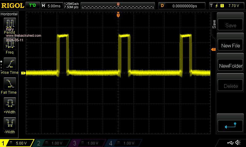 On Low mosfet Q2 : 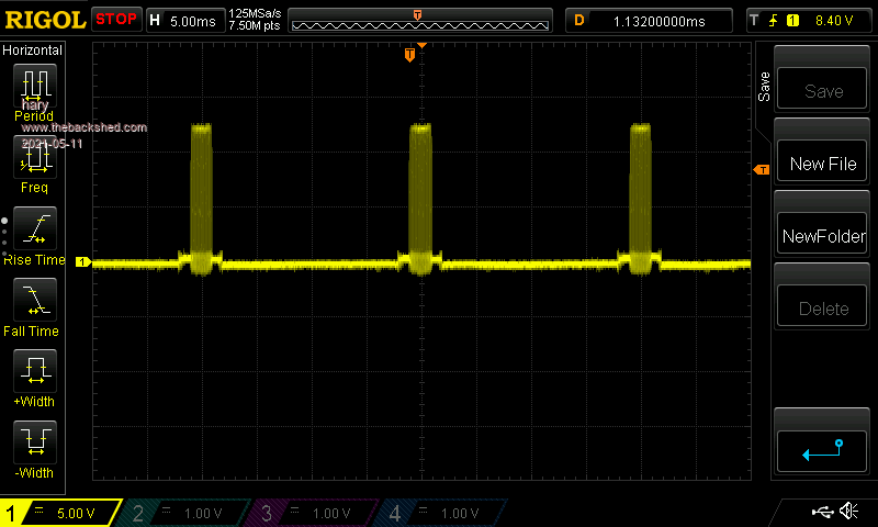 A close up look let us recognize the SPWM drive at about 25kHz if I'm right: 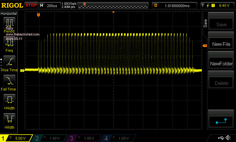 Even closer : 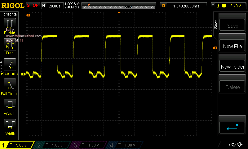 Then on the other half of the H bridge : First the High side gate (Q1) : 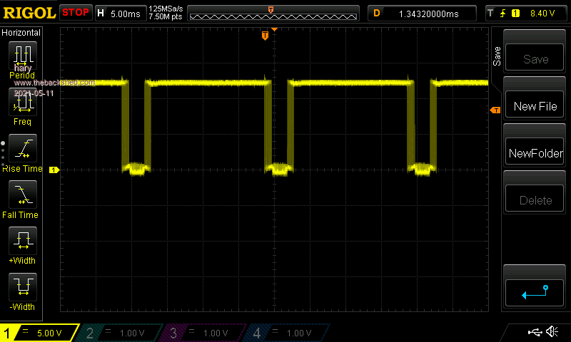 Then on the low side (Q4) : 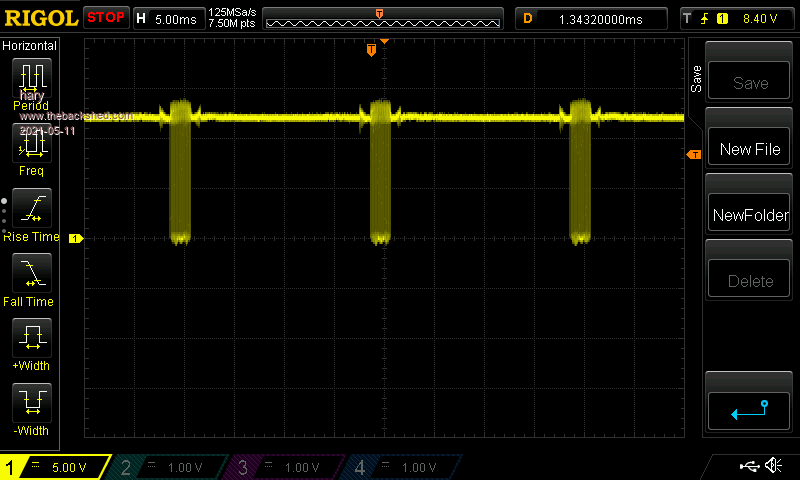 But here is what I don't understand. Why do the drive signal of the 2 last mosfets look reversed ? very strange to me. Has any one an explanation ? Do somebody see something obviously wrong ? I might have done a mistake : As it was running ok, I put a 15W bulb on the AC output, it was still ok, so I removed the safety series light bulb, it then worked for a while before entering security mode again. I removed the 15W bulb load but couldn't get back working again. I might have broken something else but don't know what. There was no smoke. Edited 2021-05-11 06:41 by hary |
||||
| wiseguy Guru Joined: 21/06/2018 Location: AustraliaPosts: 993 |
Hary, whilst I may not be able to pinpoint the exact issue with the inverter perhaps I can help you look at the information from the CRO in a better way. My guess is that 2 of the IGBTs are running at 50Hz and the other 2 are being PWM'd at the 25kHz rate. (similar to the EG8010 method of 50Hz sinewave PWM generation) You made a statement in picture 5 that the duty cycle is greater than 50%. That is not how I see it, I see a solid 50% high waveform for ~ 10mSecs. Then I see some pwm starting followed by a solid low period followed by some more PWM these 3 parts look like the other 10mSecs. Now look at picture 6 which you said is less than 50% duty cycle, again I see a solid 50% low waveform for ~ 10mSecs. Then I see some pwm starting followed by a solid high period followed by some more PWM these 3 parts look like the other 10mSecs. In picture 7 you said it was a 50Hz square trace - it looks to me like there is some PWM component at the beginning and end of the high period ? Looking at picture 4 & 5 now through new eyes tells a slightly different story. It appears to begin the PWM for the beginning of a half sinewave period then stop or inhibit the drive for a period and then a final burst of PWM at the end of a 10mS period. So it appears something is inhibiting drive for a while, is it because the (360V?) DC bus drooped below the inhibit point level or climbed beyond its upper limit, is it because the current sense of the bridge (big resistor near Q47) was triggered for a period, is it because the output sinewave became greater than the RMS max it was supposed to be. So you see there are a number of ways that the circuit can be affected to give the CRO result we see. Please note it may not be that the Vbus is too high or low, or the bridge current is beyond its max value or that the output RMS is too high, but the circuit processing these levels is lying about what it sees and that is suppressing the pwm. After reading Aarons post and taking a closer look, I agree, the opto closest to the transformers appears to more likely be the HV (360V?) regulation feedback, I assume the chip just near it is the sg3524? controller of the 360V DC circuit. By the way dont discount that the big red film capacitor might be faulty - I would have thought that the amount of the hash on the output should be filtered more than what I see, maybe that cap has seen better days ? Good luck with it. Edited 2021-05-11 08:57 by wiseguy If at first you dont succeed, I suggest you avoid sky diving.... Cheers Mike |
||||
| hary Regular Member Joined: 15/04/2019 Location: FrancePosts: 89 |
Sure you should as I'm far from being an expert. Yes, that's what I thought first after seeing these traces. The High side running at 50Hz, the low side driven at "SPWM frequency" I'm not sure we're talking about the same picture. All the traces show Vgs of the 4 N mosfets of the full H bridge. The 4 first pictures are about Q3 and Q2, the high and the low side of half the H bridge. Picture 3 and 4 beeing a close up of Picture 2. Picture 5 and 6 are respectively for Q1 and Q4 of the other half of the H bridge. For me, if Vgs=0, the mosfet is open(not conducting), when Vgs=12.5V, it's closed (conducting). At 50Hs, the period is 20ms, so none of the mosfet can be driven for a longer period of 10ms. What I can see from the trace shows the opposite. Sorry if I didn't understood what you tried to explained. I've read many time your post and I still don't catch your explanation. (I'm so sorry) Mmmm, I put only 6 pictures in my last post ! this makes the situation confused. As there was only half of the H bridge working, half of the sine had to go higher than normal to reach the AC230v at the output, and that "spike" might have been detected, thus triggering some voltage limit. Yes, that's right, it's a SG3525 and it seems to be regulated at 347-357VDC from waht I could catch with my multimeter. But if faulty, would it make Q3 and Q4 heating up and drawing some power at no load as I've seen ? I hope no making to much confusion and that you can give me some more explanation. Unfortunately, as I previously said, I might have broken something, and am now unable to run the thing and take some more measurements. Edited 2021-05-12 04:40 by hary |
||||
| wiseguy Guru Joined: 21/06/2018 Location: AustraliaPosts: 993 |
Go to the beginning of the post and count to pictures 5 & 6 down from the top. The period of a 50Hz sinewave is 20mSecs if you keep this in mind whilst trying to interpret what I said in my previous post it might make more sense. Pictures 5 & 6 both show a 10mSec period where it is stable & nothing happens therefore it is 50% of a 20mSec period. Nor am I. I only wanted to refer to pictures 5 & 6 from the beginning of your post. When you remove half of the bridge and try to run I consider all the other waveforms are possibly a bit misleading/confusing. For instance if you look at picture 5 & picture 7 they are supposedly both of Q3 gate and totally different ? Yes highly likely, the capacitor helps integrate the HF energy into a sinewave, if the capacitor is open circuit we are switching large chunks of energy into an inductor I am pretty confident there will be very fast spikes of energy possibly being absorbed by Q2 & 3 where there normally wouldn't be. The little yellow capacitor near the output wires is woefully inadequate to do the function of the big film capacitor. Ok Hary I will sign off now I'm not sure I can help further & my posts seem a bit too confusing to follow, which I am happy to take the blame for. I hope you get it fixed. Edited 2021-05-12 06:29 by wiseguy If at first you dont succeed, I suggest you avoid sky diving.... Cheers Mike |
||||
| hary Regular Member Joined: 15/04/2019 Location: FrancePosts: 89 |
But I was talking about Q3 and Q4 that were heating up (High_side of half the bridge and Low_side the other half).In that situation, I had no load, the 4 Mosfets welded in place and the light bulb in series with the DC360V fuse. I guess without the light bulb in series with the DC stage, the 2 mosfets Q3 and Q4 would have blown up. |
||||
| wiseguy Guru Joined: 21/06/2018 Location: AustraliaPosts: 993 |
Yes I made a mistake I meant to type Q3 & Q4 sorry for the confusion, not sure I was fully awake at 5.00am...... Just rereading the last few posts as I'm feeling a bit perplexed myself. Hary, I'm having trouble understanding your confusion on this point. If you only post 6 pictures in your latest post and I mention picture 7, its unlikely I'm solely referring to your last post. Lets see if we can find the correct picture another way A good hint..... you said it was "a 50Hz square trace". If you look at all the pictures in your post and their headings only the seventh picture from the top (the first picture in your last post) has that specific heading wording & you wrote it !! Voila picture numbering solved ? If finding the right picture was such hard work, you sure have your work cut out for you. This is how I look at the picture 5 it is a 50% duty cycle. 10mSeconds steady High, then 10mS pwming to low but with a "dead spot" whilst pwming low. 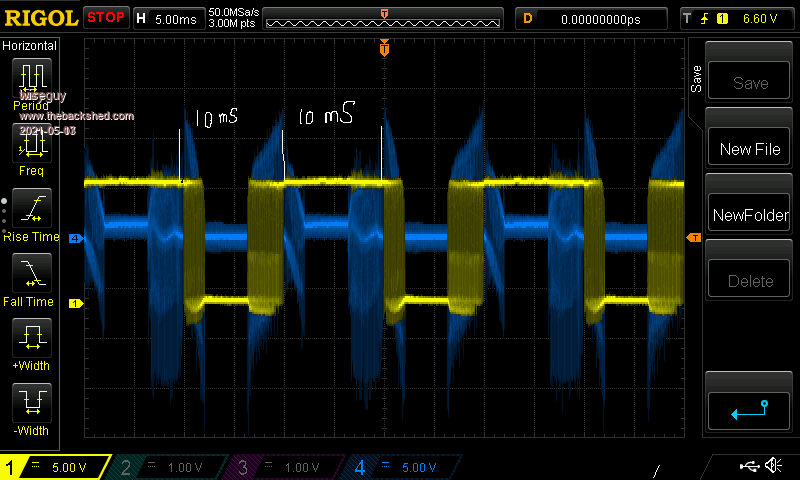 Edited 2021-05-13 00:50 by wiseguy If at first you dont succeed, I suggest you avoid sky diving.... Cheers Mike |
||||
| hary Regular Member Joined: 15/04/2019 Location: FrancePosts: 89 |
Sorry, I'm still unclear about the 2 mosfets that are meant to abnormally heat up if the capacitor would be faulty. Maybe, Q2 and Q4 (the 2 low side mosfets of each side of the H bridge) that are working at 20kHz might heat up in that case. But I'm presently talking about Q3 and Q4, as they would be conducting at the same time creating a dead short between Vbus and ground of the DC360V. 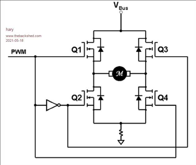 Sorry, it's sometimes difficult to explain things with worlds. |
||||
| wiseguy Guru Joined: 21/06/2018 Location: AustraliaPosts: 993 |
If I'm to help you further I prefer to do it my way and hopefully clear up some other confusing points. In picture one (the first picture in this post you refer to a 250VDC fuse, in another place you refer to it as a 360VDC fuse and also elsewhere as a 200VDC line - does it also have a current rating - a fuse normally is referred to by its current rating in Amps ? Elsewhere in the post you refer to the unit as a 230VAC inverter but you were looking at the 220VAC lines ? You also refer to the spwm as 20kHz 21kHz and 25kHz in various places. It would be helpful to avoid confusion if you are more consistent in your posts Noneya suggested an approach and it appears he didn't even get the courtesy of a reply. "As you can see, it's larger than 50% duty cycle. I thus think it was obvious that Q3 was overlapping Q4 duty cycle time, and the explanation was clear." Well no this whole statement is ambiguous and guesswork at its best. If you approach something with a closed mind you probably see what you want and then are liable to ignore details and bend the theory to suit your argument. If Q3 & Q4 have overlapping drives is it because the control circuitry has forgotten its task or is the signal being corrupted between where it is generated from and where it is applied to the IGBT ? Hint trace the signal back. Secondly, normally if we refer to duty cycle, it usually applies to a single complete transition/cycle of an on and an off time event and the ratio between those 2 states. If you look at pictures 9 & 10 there are a number of pulses with a varying duty cycle that make up a portion of the sinewave that is trying to be generated, each has a duty cycle that is consistently varying. The whole sinewave is created through a mixture of HF and LF waveforms on all 4 gates that interact to create a sinewave. Looking at one gate with partial 50HZ and HF PWM content at different times and talking about duty cycle is in it self confusing and misleading. So lets revisit the statement "As you can see, it's larger than 50% duty cycle. I thus think it was obvious that Q3 was overlapping Q4 duty cycle time, and the explanation was clear.' Sorry still not obvious nor clear to me and I need to see all 4 gate waveforms and relative to each other before I can help further In one of my first posts I suggested ":Maybe you can remove VBus from the top of the H bridge and get a much better look at the 4 different gate drives safely with less pollution from whatever fault may exist. It would be preferable to stop the Dc/Dc from generating the VBus but you may have to fool the microcontroller that VBus is ok or it might inhibit drive." I still think it is a good approach. The 200/250/360VDC line should be broken before it gets to the IGBTs, dont break the HVDC line before the HVDC regulation feedback. If there is monitoring of the HVDC line by the control circuitry this should still function and the HVDC line wont go rampant if it still has the control loop connected. "High DC voltage was about 347-357VDC, and AC output was about AC269V with a non RMS voltmeter and with half of the full H bridge missing, so probably half of the 50Hz sine". Probablys are totally misleading and probably dont help at all, next time put a CRO trace at the 230V? AC output and show what is happening, an RMS/non-RMS meter is next to useless in this application, except for known DC measurements, and then not DC with lots of ripple or hash. Lastly in picture 4 the HF content on the 50Hz line is very high and "appears" to be ~ 20V of "hash". I am sure this should not be there, it is usually removed by the big red capacitor and smaller yellow capacitor, it is also possible that through improper driving of the IGBTs could induce the hash. I dont want to enter into a theoretical discussion about whether the capacitor should or could cause Q3 & Q4 to heat up and why. It was more a suggestion that it is unclear what effect or effects it could have apart from not filtering all the hash on the AC output. Sometimes a fault can have multiple effects that are hard to get your head around but they all magically disappear when the faulty part is found and fixed. Maybe I cant help further - this has to be one of my least rewarding experiences I have had trying to help some one who ignores most questions and suggestions and wants to tread their own path. Good Luck with it. Edited 2021-05-18 08:15 by wiseguy If at first you dont succeed, I suggest you avoid sky diving.... Cheers Mike |
||||
| Revlac Guru Joined: 31/12/2016 Location: AustraliaPosts: 961 |
@Hary, There is a diagram in this manual that night be helpful. Search Axpert MKS 1-3KVA Service manual 20130611.pdf I think it is on the AEVA Also the choke on some of these will produce heat even when no load is connected. I don't mind helping people but I am out of ideas with this now, best of luck with it. Cheers Aaron Off The Grid |
||||
| hary Regular Member Joined: 15/04/2019 Location: FrancePosts: 89 |
First, to everybody, I want to excuse myself if I misbehave. Just keep in mind that english isn't my mother's language, and I'm not an electronic guy. I'm just trying to find out and learn things the way I can. @Revlac, I think I found the pdf you were referring to : Axpert MKS 1-3KVA Service manual 20130611.pdf At least I have a basic schematic diagram to work on and properly name things. @wiseguy. I'll try to be more accurate in my writing and pay more attention to advices. You said : "In one of my first posts I suggested ":Maybe you can remove VBus from the top of the H bridge and get a much better look at the 4 different gate drives safely with less pollution from whatever fault may exist. It would be preferable to stop the Dc/Dc from generating the VBus but you may have to fool the microcontroller that VBus is ok or it might inhibit drive." I still think it is a good approach. The 200/250/360VDC line should be broken before it gets to the IGBTs, dont break the HVDC line before the HVDC regulation feedback. If there is monitoring of the HVDC line by the control circuitry this should still function and the HVDC line wont go rampant if it still has the control loop connected." I think after breaking the HVDC, I must remove the 4 mosfets before using the 4 probes on the 4 gates of the DC TO AC inverter full-bridge ? (As the CRO has the same GND for all probe) |
||||
| wiseguy Guru Joined: 21/06/2018 Location: AustraliaPosts: 993 |
Sorry Hary I missed this last line - it initially just looked like part of my quote. Are they 4 x Mosfets or 4 x IGBTs? I shall refer to them as XXs until we know. When the V+ (360V) is removed from the bridge the Nodes between the high side and low side XXs should no longer be jumping between V+ and Gnd, use a voltmeter set to DC and confirm that the vode between the high/low XX parts is at zero V or very close to it. If you get a different result tell us about it. The fact that you may have one or more dead XXs it might be a good idea to remove them all before looking at the gate waveforms to ensure good integrity of the drive. If the XXs all appear ok you should be able to scope the upper and lower Gate drives with one probe ground on the HV- and the other grounded to the source/emitter of the upper device. One by one you should also be able to load the Gates with a 4n7 in parallel with a 470R resistor and see that the waveform is almost the same as without the load. If one gate signal collapses to a much lower drive then it needs further investigating. The resistor will get hot fairly quickly so don't take to long checking. If at first you dont succeed, I suggest you avoid sky diving.... Cheers Mike |
||||
| hary Regular Member Joined: 15/04/2019 Location: FrancePosts: 89 |
Hi wiseguy and thanks for keeping motivated for still providing help. They are 26N50P mosfets As I said before, I must have done a mistake somewhere as now I can't get HV mosfets drives signal anymore and DC Vbus+ doesn't exceed DC130V now.(should be DC360V or so). It's doing so since I last was able to light up a small light bulb on the AC side with only half of the bridge's mosfets (the other half bridge's mosfets were removed). Doing so must have destroyed something somewhere ! The indication you give involve many guesses from my side since I don't have all the required knowledge. My CRO indicates a 300V max, so I'm a little afraid I would blow it up doing some wrong measurement. It's surely a good learning project, but with no proper schematics and too poor knowledge, it might be a too difficult task for now  . . |
||||
