
|
|
Forum Index : Electronics : H-Bridge Dead-time Inserter
| Page 1 of 2 |
|||||
| Author | Message | ||||
| Solar Mike Guru Joined: 08/02/2015 Location: New ZealandPosts: 1228 |
AS described, this topic is to show differing circuits for inserting the required dead time into the 20kHz spwm and 50hz signals for driving opto coupled H-Bridges. There are a number of forum members designing new synchronous modular H-Bridges, myself included, so I thought I would present a few dead time generators that can connect direct to the IO pins of the CPU and create some discussion as to the best way to do it. My inverter needs a single cross-coupled drive signal for its simulated opto inputs on each 1/2 bridge; the 1/2 bridges can be paralleled to increase the output power, so I could have 3-4 wired together. Each opto signal needs 8-10 mA, thus up to 40 mA drive current from a totem pole type driver, normal logic gates can manage perhaps a single opto, certainly not 4. This design uses the mini logic gates in the output each with 32 mA drive, so 2 gates in parallel will happily do what I want. I looked at having one or two RC networks as the dead time delay, but having used this on previous designs, its easy to setup with the right test gear, BUT its not repeatable, the delay timing varies with temperature and the IC being used, so have rejected the idea of RC delay for timing. There are a number of silicon delay lines available that have taps where you can select what delay is required and they are accurate. This design used two delay lines, one for each 1/2 Bridge signal. The delay is inserted in the trailing and leading edges of the pwm by action of the XOR gates, the following NOR gates act as an inverting buffer and Enable input. Though I could put something like this on a small pcb that plugs into the main CPU board. 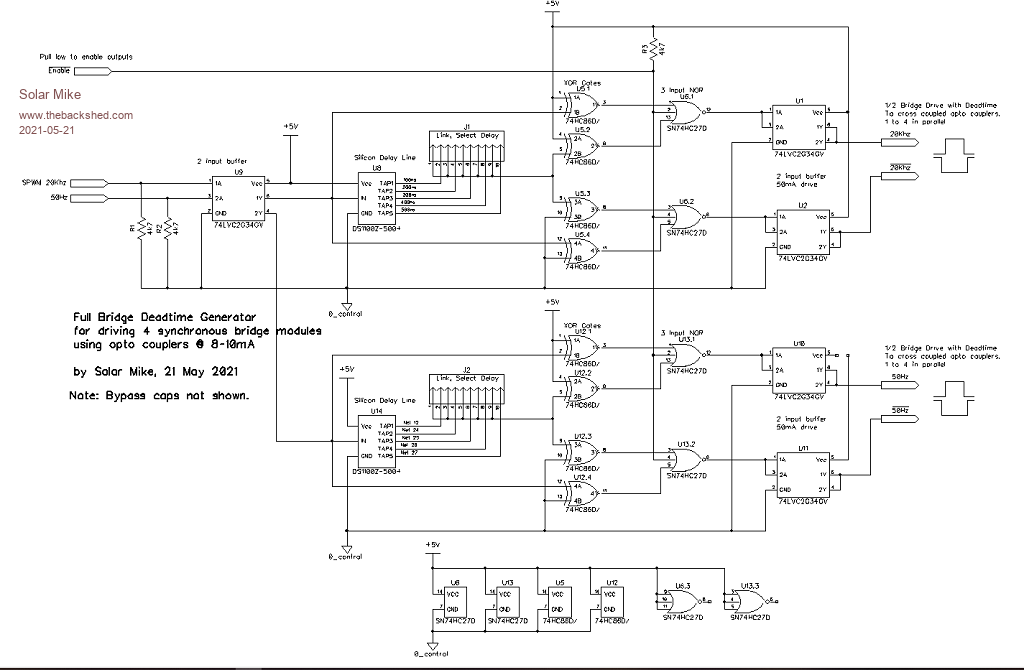 BridgeDriver.pdf Comments.... Mike Edited 2021-05-21 20:13 by Solar Mike |
||||
| Warpspeed Guru Joined: 09/08/2007 Location: AustraliaPosts: 4406 |
If you are still planning to use opto couplers (a good idea) there will still be some random differences in opto delays with time, temperature, manufacturer etc... I still like the cross coupled inverse LED driver circuit with a dead time capacitor, plus you get shoot through protection for free. Cheers, �Tony. |
||||
| Solar Mike Guru Joined: 08/02/2015 Location: New ZealandPosts: 1228 |
The newer simulated opto couplers that am now using have no where near the random differences as exhibited by the old style opto's, they are extremely close in tolerance between devices and hardly affected by temperature variations. When multiple half bridges are paralleled, having multiple capacitors each with a differing timing just exasperates the problem, great if just a single H-Bridge is being used. Cheers Mike Edited 2021-05-22 09:00 by Solar Mike |
||||
| poida Guru Joined: 02/02/2017 Location: AustraliaPosts: 1480 |
if I needed this, and I wanted a simple solution, I would use one IC costing $1.70, and one decouple cap. Input is PWM and ground ouput is the low and high side drive, with 500ns DT. The chip is the IRS2004, 0.6A output. Or the IR2184 but they cost $6. No need for it's 2A drive capability. Connect Vb to Vcc and Vs to ground. The single PWM pulse train will now be the complimentary pulse train with dead time. 0.6A output at the voltage of Vcc 2 components. wronger than a phone book full of wrong phone numbers |
||||
| Solar Mike Guru Joined: 08/02/2015 Location: New ZealandPosts: 1228 |
Certainly cannot beat that for simplicity, I did look at some of the various half bridge drivers and that maybe the easiest solution, however 500ns delay is a little long when the smallest spwm pulse is approx 5uS. Would prefer something variable, so would rule that device out, but there maybe others with lower drive output that allow variable timing; certainly the higher current versions do this like the IR21844 even if they cost more. Cheers Mike |
||||
| Solar Mike Guru Joined: 08/02/2015 Location: New ZealandPosts: 1228 |
Here is another alternative, simpler than the first delay line example, using a single RC delay with independent adjustment of leading and trailing delays, and the components are cheap. It is not repeatable in that every build would have to be setup with a scope for the correct timing; which will also change with temperature. 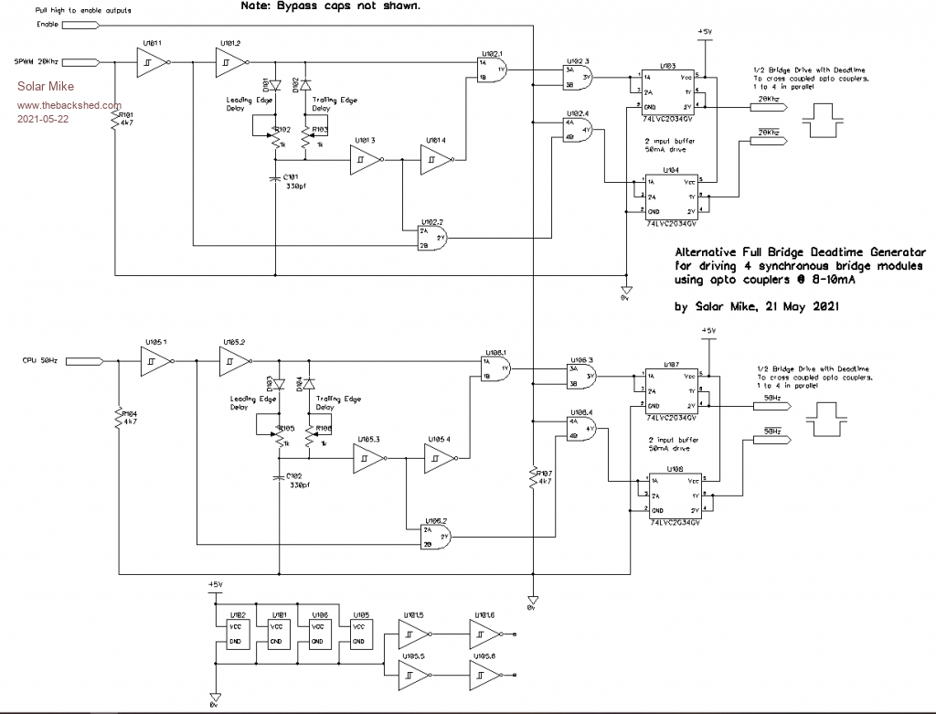 Cheers Mike |
||||
| tinyt Guru Joined: 12/11/2017 Location: United StatesPosts: 561 |
How about using COG/NPO dielectric capacitors to minimize drift due to temperature. Maybe drift introduced by the diodes can be compensated by PTC or NTC resistors. |
||||
| Solar Mike Guru Joined: 08/02/2015 Location: New ZealandPosts: 1228 |
Good point, there is also the schmitt trigger trip points changing with differing devices. Have spent last couple of hours looking for a single chip solution that has a good adjustable range in dead time settings, the modern isolated drivers like the Si8234BB-D-IS1 series would be ideal; BUT no one has any for sale, everything is on back order until the end of the year or later, I have some here but they are the faster H versions that I use in the PV controllers and wouldnt be suitable. The only chip I can locate that IS actually available to purchase is the LM5106 , this older inexpensive device would work well as it has a range approx 85 - 550 nSec by altering a resistor, powered from 12v source and under voltage lock out. Presumably the upper H0 VB can also be also powered from the 12v supply and Hs pin to 0v, this is unproven as they may not be on separate dies inside the package. Element14 have them in stock, however have to get $50 worth to get free shipping, so would have to wait awhile on those until I need more bits, or locate an alternative supplier. Cheers Mike Edited 2021-05-22 21:54 by Solar Mike |
||||
| wiseguy Guru Joined: 21/06/2018 Location: AustraliaPosts: 1297 |
I think the The UCC21520 is very worthy of consideration in the pursuit of deadtime control tweaking. It also has very good (low) propagation delay and rise/fall times. ucc21520.pdf The overview 8.1 on pge 19 reveals its highlights/features. and application note tidudj9.pdf Give a good insight into dead time generation, which is built in to this gate drive isolator/buffer with a single timing resistor and small capacitor for noise abatement. The resistor RDT generates a time in nanoseconds which is 10 x RDT's value in KOhms. So for 10K it will generate 100nS. Adjustment range is from 0.5K to 500KOhms which is an adjustment range of 5nS to 5uSecs. I think for 20kHz operation deadtime could be preset to a known safe value ie 200nSecs for a given topology and perhaps sleep should not be lost by the fact that it could have been reduced by another 10 or 30 nSecs. If designs are going to tighten up (minimise dead time) then the parts lists will have to be quite specific in these critical output stage areas, freedom of choosing parts at hand will be reduced, as close enough may not be good enough.. A lot of constructors dont have access to accurate CROs and test equipment required for individual tweaking. I guess you could always put a pot on it and tweak until you hear a loud bang and then back it off ~ 20%  - and replace some FET's - and replace some FET'sEdited 2021-05-23 01:08 by wiseguy If at first you dont succeed, I suggest you avoid sky diving.... Cheers Mike |
||||
| wiseguy Guru Joined: 21/06/2018 Location: AustraliaPosts: 1297 |
Mike I would like to put down some thoughts on deadtime and ask you for some comments to either support or enlighten my thinking. Having some more time to think about deadtime perhaps it might be helpful to define what it is, why its needed & its merits and otherwise. Deadtime is the time/safety margin involved in trying to avoid catastrophic shoot through current. If we consider a half bridge with upper and lower mosfets if both FETs are ever on at the same instant in time the supply rail is essentially shorted through the FETs and they self destruct. In the quest to ensure this never happens we insert a safety margin "deadtime" to ensure one FET is off before the other turns on and vice versa. The UCC21520 device above only controls the on time delay for the upper/lower FET's this ensures the opposite FET has had enough time to cease conducting before the other FET turns on. I do not see a merit in controlling the leading edge turn on and the trailing edge turn off times, as only one should be required? Positives of just enough Dead Time, Fets are protected from shoot through. Negatives from too much dead time, FET body diode conducts during dead time and due to the forward voltage drop generates unwanted heat, PWM on time from controller is reduced which reduces maximum output - mainly noticed when Mains output droops earlier than expected as battery discharges. How to explore and adjust deadtime safely with the UCC21520 without a CRO or similar means of measurement. For an H bridge converter remove/isolate Bulk capacitors from Power board. disconnect one side of transformer primary or choke. Insert a resistor of 1 - 10 Ohms in the positive H Bridge supply lead, set input voltage to nominal input voltage (48?). With a 50K Pot wired to the deadtime adjustment pin, ensure it is at the 50K setting (500nSecs) and apply PWM from the controller. Now if we adjust the 50K setting lower we will get to a point where input current rapidly increases, back off the pot setting slightly to just below the increase. Now do the same for the other half of the H bridge. Power down and read the pot value/s (lets assume it is say 12K). The minimum dead time is therefore 120nSecs. I would suggest adding no less than 20 and no more than 50nSecs by increasing the Pot by 2K to 5K from the measured value and replace the pot with a fixed resistor. What affects dead time margin in a given design topology, The Mosfet type No chosen and the parameter tolerance spread in the chosen Mosfet, the gate resistor/s value, voltage chosen for 12/15V gate drive supply, transistors types used for the buffer, opto or isolator used with its own parameters etc. This is why it is hard to create a flexible design that allows some discretion of parts used and yet not have too much wasted deadtime. Edited 2021-05-23 10:49 by wiseguy If at first you dont succeed, I suggest you avoid sky diving.... Cheers Mike |
||||
| Solar Mike Guru Joined: 08/02/2015 Location: New ZealandPosts: 1228 |
Yes Agree, it wasn't on my list as no one has any stock, until next year; have used the UCC21521DW version in the PV charge controllers, same spec's has an "Enable" rather that "Disable" input. The only readily available device is the LM5106 or build something from logic gates as described. Cheers Mike |
||||
| Solar Mike Guru Joined: 08/02/2015 Location: New ZealandPosts: 1228 |
Good description Correct, that's how it normally works, you control the turn On of the device that was previously Off, at the leading and trailing edges. My circuit #2 allows a different On time at each transition, if required, normally the delay is constant and differing gate bias resistors allow extra finesse. Yes, mainly at low modulation levels say 10%, then too high a dead time introduce distortion products as its a high percentage of the mosfets On time. Definitely remove the big electro's, easy to do with the cap's on a separate pcb module. Perhaps it might work that way, seems reasonable, bit of an unknown until someone tries it out...  Basically its dependent on the time for one mosfet to stop conduction, so the other can turn on; faster you can turn them off, sooner the others can be enabled. The dumping of the On mosfet gate charge depends on everything you have said including the layout and lumped inductance in the gate-source circuit back to the driver chip. I would say the layout and driver chip would have the most effect, get that right would be a good start. Cheers Mike |
||||
Revlac Guru Joined: 31/12/2016 Location: AustraliaPosts: 1282 |
Some time back I read an appnote about switching IGBT's and dead time, The application was for a welder, and that there was some overlap in switching, apparently some was used was because the long length on the welding leads and the choke had to handle it. At the time of reading it made sense for use in a welder, now it doesn't seem so good for an inverter by the looks of it. After reading the notes posted earlier, its a bit easier to understand the workings and use of dead time, still not easy for the first time builder without some test gear though.  Good info here, Thanks. Cheers Aaron Off The Grid |
||||
| wiseguy Guru Joined: 21/06/2018 Location: AustraliaPosts: 1297 |
Whoops, the first two buttons I normally press with Digikey is the "active" and the "in stock" before any further filtering - no point in getting excited if its not in stock or about to be obsoleted. Must have overlooked/forgotten to do this, I see lead times of ~ 35 Weeks sheesh dammit. And its such a good part too........ Also, thanks for your considered responses to my thoughts. If at first you dont succeed, I suggest you avoid sky diving.... Cheers Mike |
||||
| nickskethisniks Guru Joined: 17/10/2017 Location: BelgiumPosts: 481 |
I see manufacturers specify their MOSFETs turn on/off timing with a certain load for instance 75A and Vds 64V. Would a load or no-load matter a lot when performing such tests? Would an adjustable software dead time be an option? |
||||
| Solar Mike Guru Joined: 08/02/2015 Location: New ZealandPosts: 1228 |
A mosfets transconductance changes with load and voltage, so they generally specify set load points for their published specs. Here's some info Its Complicated I wouldn't trust the CPU timers to produce a constant or varying for that matter any form of dead time, the PIC CPU's have dead time settings in some of the PWM outputs, but looking at the wave forms on a scope during power down they go all to hell; too risky. |
||||
| Solar Mike Guru Joined: 08/02/2015 Location: New ZealandPosts: 1228 |
Looking in RS or Element14 online, seems 50% of everything is now on back order until end of the year or later in 2022, even the auto industry is getting affected because of chip and component shortages. Will just have to come up with inventive ways to use what we have. Mike |
||||
| Solar Mike Guru Joined: 08/02/2015 Location: New ZealandPosts: 1228 |
Update Mouser have stocks of the UCC21521DW 1/2 bridge drivers, these are same as the ..21520 but with an enable rather than disable input, the DW or DWR suffix devices have 8v under voltage lock out, not cheap and not thru hole, none of these newer chips are available in thru hole now. Edit: Texas Instruments store has 70 in stock, good price and postage. Store Very tempted to use these for the CPU variable DTime, as they are very versatile in that having dual internal isolated dies, can be used as dual HSide, LSide or HBridge to drive mosfets directly. Mike Edited 2021-05-24 12:46 by Solar Mike |
||||
| Solar Mike Guru Joined: 08/02/2015 Location: New ZealandPosts: 1228 |
Will make this as a small module for plugging into the CPU controller board. As the chip shortage worsens, its getting impossible to get anything exotic, so will create two modules with different components, should some become unavailable. First build uses the Si8234AB-D-IS1 driver for the variable dead time generator, this isn't my preferred device, but none of the others are available until 2022. 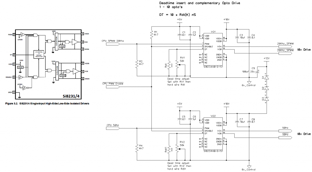 Cheers Mike |
||||
| Solar Mike Guru Joined: 08/02/2015 Location: New ZealandPosts: 1228 |
2nd version uses the LM5106MM, these seem readily available at the moment and quite cheap. Enable input is Active High, other is active Low, will make them both 1 = on in final build. 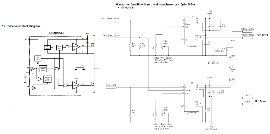 Cheers Mike |
||||
| Page 1 of 2 |
|||||
| The Back Shed's forum code is written, and hosted, in Australia. | © JAQ Software 2026 |
