| Author |
Message |
Solar Mike
Guru

Joined: 08/02/2015
Location: New ZealandPosts: 1123 |
| Posted: 11:28am 04 Feb 2023 |
 Copy link to clipboard Copy link to clipboard |
 Print this post |
|
Its been a good while since I looked in my box of inverter half finished projects, specifically the PI Pico RP2040 Controller; the original version can be improved upon and implemented in a more modular fashion. With JLCPCB lowering their prices of 100mm footprint 4 layer boards to $7, it makes better sense to alter the circuit somewhat and redesign for 4 layers, achieving better noise and EMI performance.
So a new schematic and PCB, the new PCB has the power supplies and AC current\voltage sensing split off on their own "Hat" 2 layer modules 100 x 50mm, these sit above the main 4-layer CPU board. I can re-use the PSU module in other projects as its somewhat generic with its 12, 5, 3.3 volt outputs.
The new controller still uses the PIO to create the SPWM wave form, but I have ditched the PIO generated dead-time delays, instead have opted for using 2 tiny 1/2 bridge chips each with variable dead-time adjustment. Each 1/2 bridge chip is used in a complementary low side driver format to allow multiples of "E-Opto" isolated mosfet drivers in an interlock arrangement on the 1/2 bridge mosfet power modules. These 100 x 100mm boards can be connected in daisy-chain for whatever power output is required.
Still want to use "Feed-Forward" DC battery voltage sensing to control AC output and is simply done by the CPU selecting one row in a table of pre-generated SPWM lookup sine values based on a modulation depth, there are hundreds of rows of 180 degree value range to choose from. After every 50 Hz period a new row can be selected depending on voltage.
I will start posting the schematics with comments then the PCB layouts.
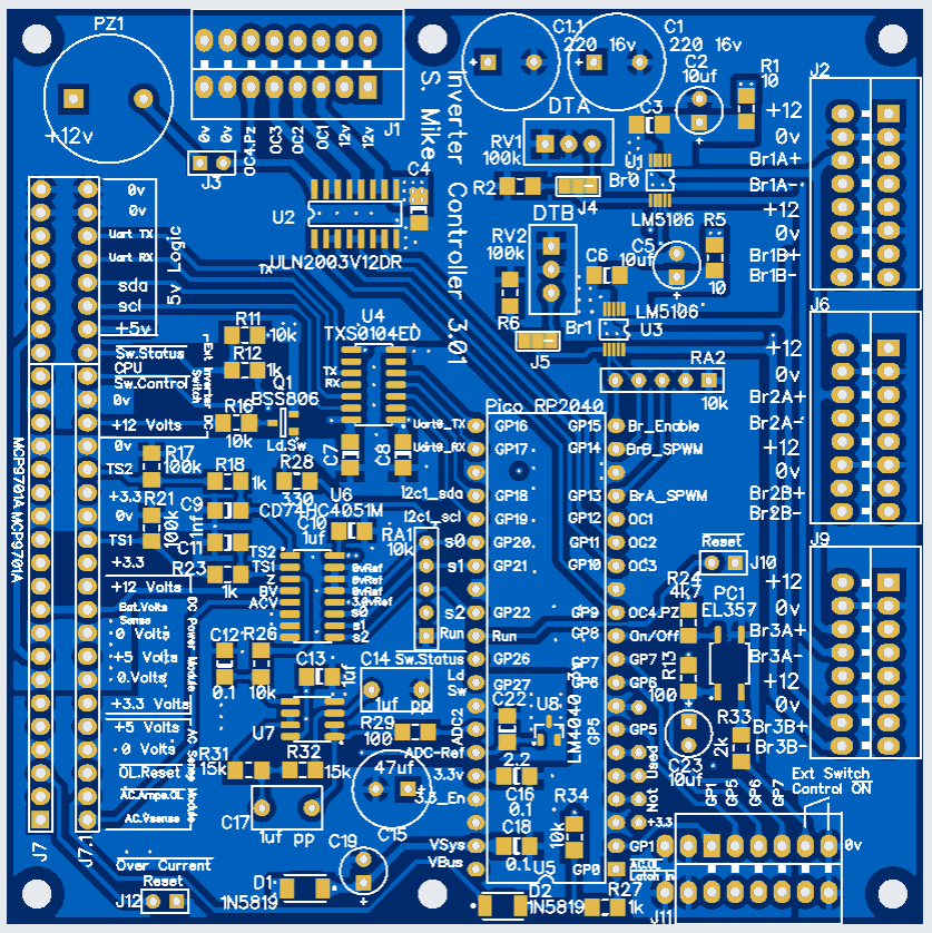
CPU:
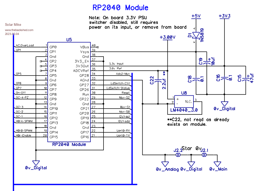
Here we see the RP2040 module connections, not all pins are used, some are output to terminal strip for generic use. The on board switching PSU has been turned off and replaced by analog DC inputs, noting that a 5v rail has to be present in order to disable the PSU chip, or it could be unsoldered from the pcb.
Getting late, continue tomorrow...
Mike
Edited 2023-02-05 05:54 by Solar Mike |
| |
Solar Mike
Guru
Joined: 08/02/2015
Location: New ZealandPosts: 1123 |
| Posted: 01:54am 05 Feb 2023 |
Copy link to clipboard |
Print this post |
|
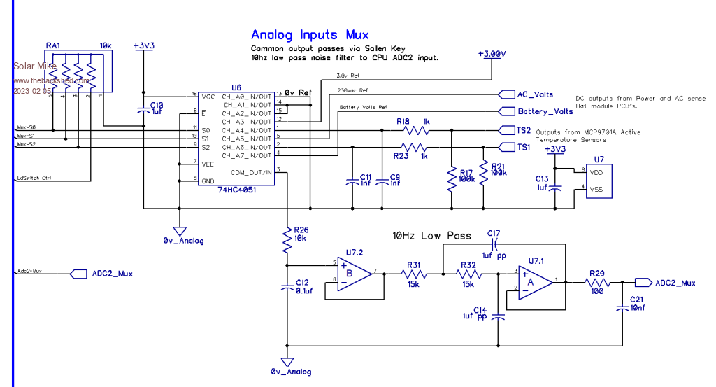
Continuing with the schematic, here is the analog IO part, the Pico doesn't have many ADC inputs so it's easier to implement additional ADC's by using a Mux, here I have used the HC4051 with 8 inputs and 1 out, a 10 Hz Sallen-Key low pass filter is used on the mux output to get rid of any noise prior to the CPU input.
H-Bridge Drive:
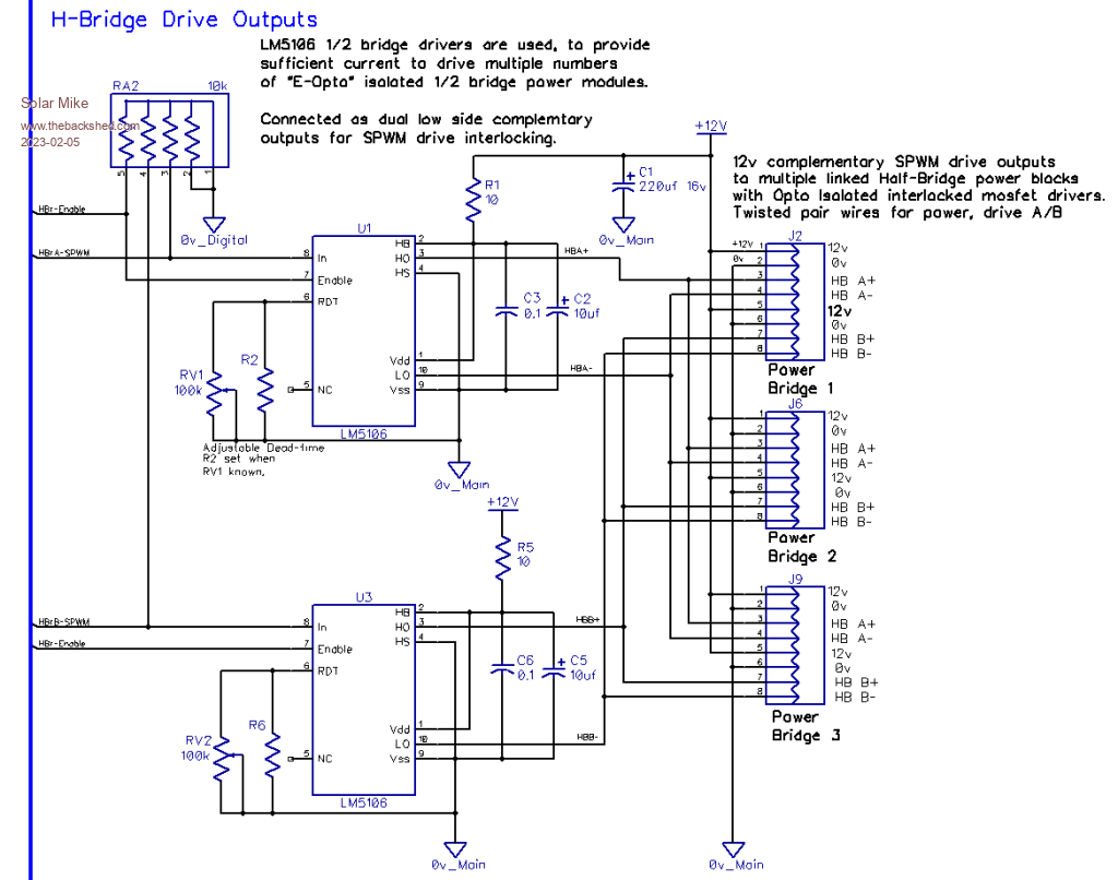
The Pico PIO outputs two SPWM modulation signals in the 35 Khz region, one for each 1/2 bridge power stage, if say the LHS HB-A is switching the other RH side HB-B has a logic 0 input, so its top H0 is off and the bottom L0 mosfet output is turned on, allowing a diagonal conduction through the transformer winding; and vice versa for the following 100 Hz half cycle.
The LM5106 drivers have plenty of capacity to drive multiple 1/2 Bridge power boards using the complementary H0-L0 channels as drive signals to the "E-Opto" inputs of each power module - which are arranged in an interlock, so cross conduction in the mosfets can never occur; they also lockout any outputs on low voltage and share a common "Enable" input signal from the CPU. The dead-time adjusters RV1\2 once set can be replaced by fixed resistors.
I have only allowed for 3 full power bridge modules on spring sockets J2,6,9, however they can be daisy-chained from a single drive socket if required.
Other IO:
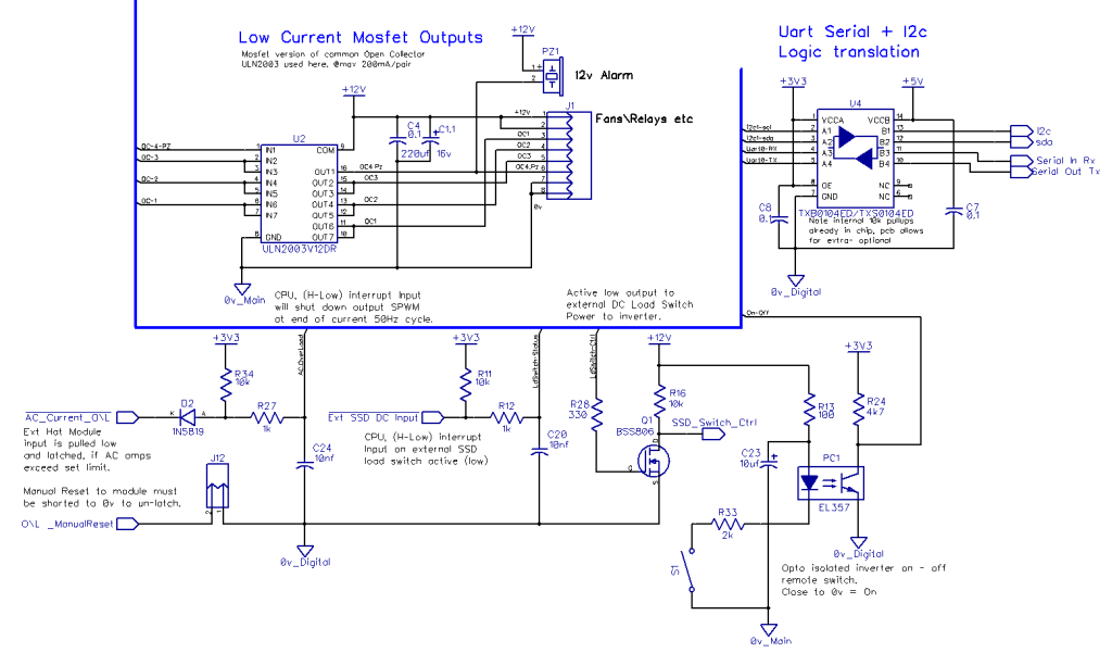
The mosfet version of the common open collector ULN2003 driver is used here for low power fans or relay outputs, saves a lot of components using them.
Optional serial or I2c data connection to a 5v LCD display is provided by a TXS0104 logic translator.
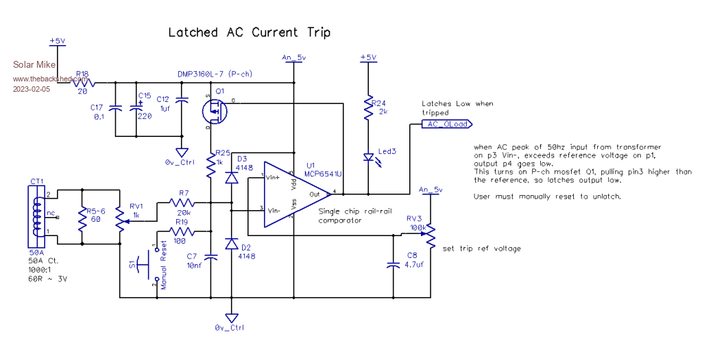
A latched AC current overload input is used to shut down the inverter by the CPU at the end of the current 50 Hz mains cycle, so magnetic flux remnants are not left in the transformer core.
I'm using my 300A SSR to switch power to the inverter, so an output is provided for that.
The main on\off switch is via an opto-coupler, allowing longer leads to the switch.
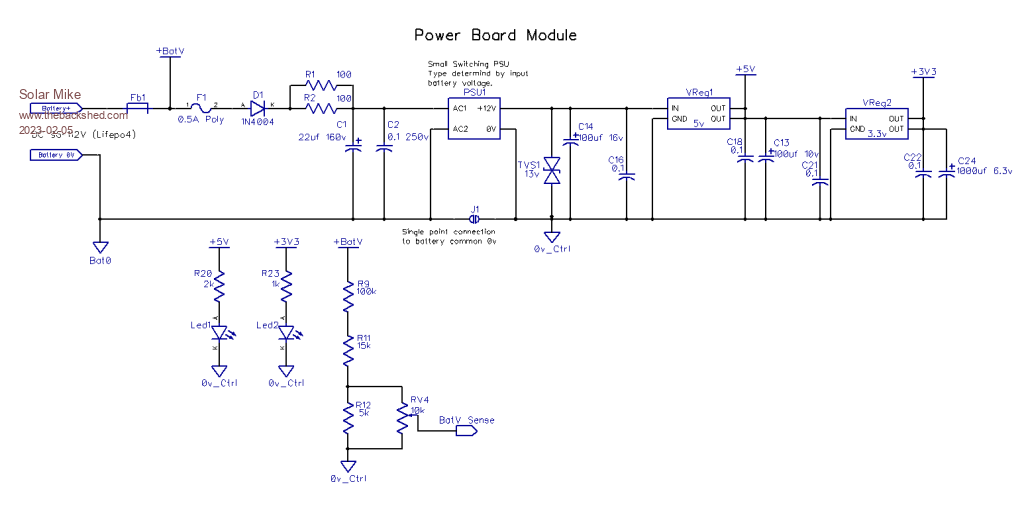
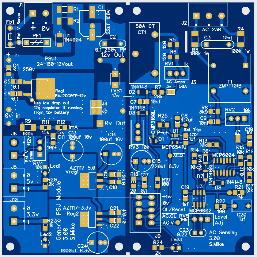
DC Power PCB:
Small 50 x 100 pcb sits above the main CPU board and contains a 12v switching supply of various sorts depending on battery voltage input and analog 5v, 3.3v regulators.
AC Sense PCB:
50 x 100 PC, sits above the DC power board and has both AC current CT and voltage transformers.
The output of the 50A CT is set to approx 3v by selection of suitable burden resistor R5-6, a rail\rail single comparator detects the positive going peak of each 50 Hz AC and if its voltage input on P3 exceeds the set point RV3 on P1, the output is pulled to 0v, turning on Led3, biasing on P-Ch mosfet Q1 and further pulling the input P3 to 5V, latching the output low. A manual reset after the overload event reverses the operation.
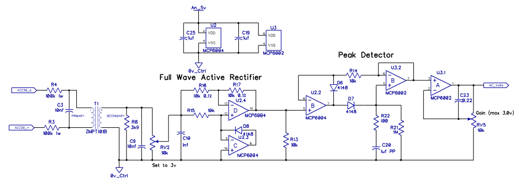
I never intended to measure the RMS AC current and display it, so have not included any circuitry to do that, its easier to use cheap dedicated display modules that show AC volts\Current\Power\Frequency etc clipped to the inverter front panel.
However I do want to know the AC voltage with some accuracy and have used an active precision full wave rectifier followed by a continuous peak detector
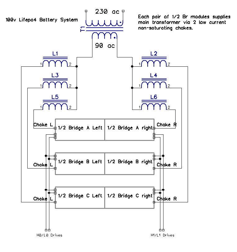
Here is a block dia of the main inverter output:
The identical left and right 1/2 Bridge power modules each contain 2 parallel mosfets in each H0 - L0 half + 2 large storage electro's, groups of these pairs are daisy-chained for drive input and link to the main transformer by a small powdered iron core, conservatively allowing 50 amps current per pair, modules can be added to achieve the desired power output; that's the theory anyway
Will generate the pcb gerbers next and show the layouts.
Cheers
Mike |
| |
Solar Mike
Guru
Joined: 08/02/2015
Location: New ZealandPosts: 1123 |
| Posted: 05:03am 05 Feb 2023 |
Copy link to clipboard |
Print this post |
|
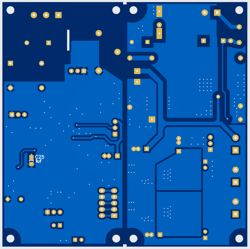
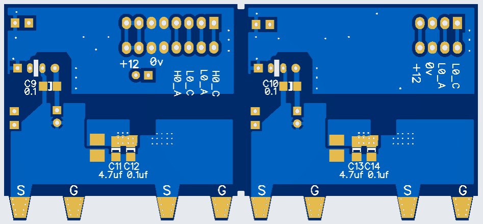
DC Power and AC Sense PCB's; both are on a 100 x 100 PCB, manually cut using a sharp knife to score both sides through the center of the small notches, then snap in half.
They stack above each other and the main CPU board.
Top:
Bottom:
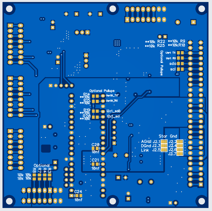
4-Layer CPU 100x100 Top:
Bottom:
Power modules next... |
| |
Solar Mike
Guru
Joined: 08/02/2015
Location: New ZealandPosts: 1123 |
| Posted: 05:07am 06 Feb 2023 |
Copy link to clipboard |
Print this post |
|
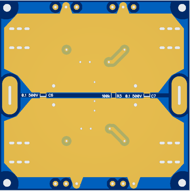
Here is the layout for one 1/2Bridge power module, it uses four mosfets, two in each H0, L0 positions, they mount off the pcb bolted to the case back panel of 5mm thick alloy.
A minimum of two modules are required to create a single H-Bridge, copper bars bolt between modules for +100 and 0v.
I haven't a circuit for this part as its more mechanical and somewhat self explanatory. Obviously components rated for whatever battery voltage will be used, snubber components are there incase, I will be leaving them off initially.
Top 100 x 100:
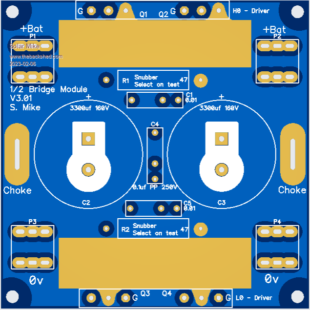
Bottom:
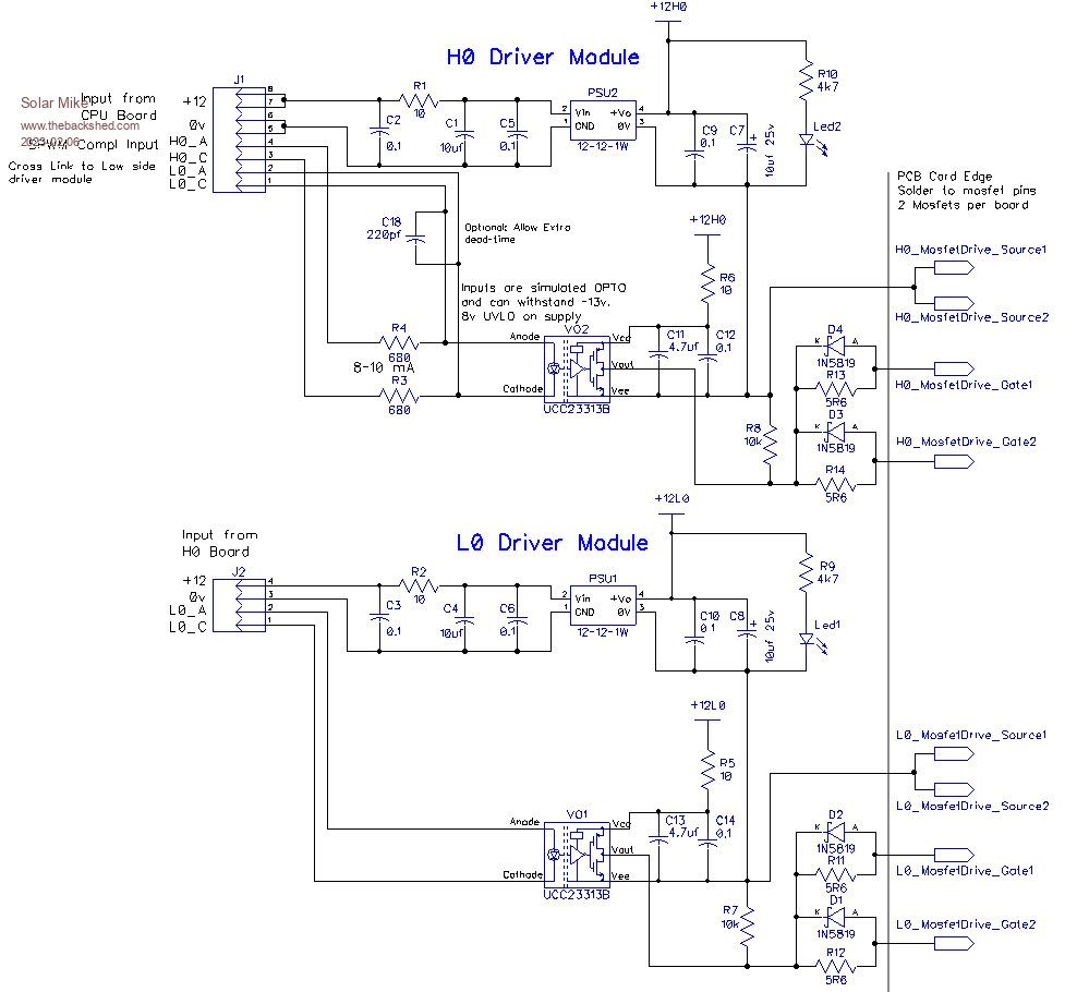
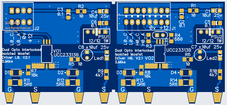
Power Board Mosfet Drivers:
Small 45 x 45mm pcb's containing the "E-Opto" isolated drivers blob solder vertically directly across the mosfet pins, this achieves short direct mosfet drive signal paths.
Each module has its own 1 watt 12-12v isolated PSU for total isolation back to the main CPU board. The pcb's are 1.2mm thick and easily cut in half to give the 2 boards, the lower L0 driver links to the H0 driver by twisted pair wires.
Note the lower L0 SPWM drive is reversed from the H0, thus creating the inter-lock drive, there is provision for adding a dead-time capacitor, C15, I won't be using it as the dead-time is created on the CPU board.
Schematic:
Both Boards:
I will be sending this lot away to get PCB's in about 4 weeks, so will be some time before the build starts.
Cheers
Mike |
| |
