Notice. New forum software under development. It's going to miss a few functions and look a bit ugly for a while, but I'm working on it full time now as the old forum was too unstable. Couple days, all good. If you notice any issues, please contact me.
Murphy's friend Guru Joined: 04/10/2019 Location: AustraliaPosts: 678
Posted: 07:33am 14 Oct 2023
Copy link to clipboard
Print this post
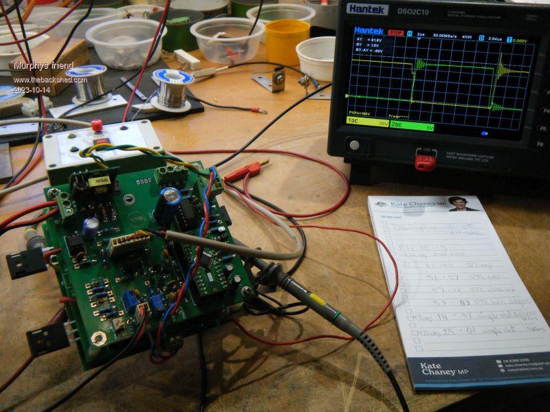
I am trying to understand the mysterious "dead time" of inverters. For that I got myself a DSO which allows me to see what happens when the mosfets switch over.
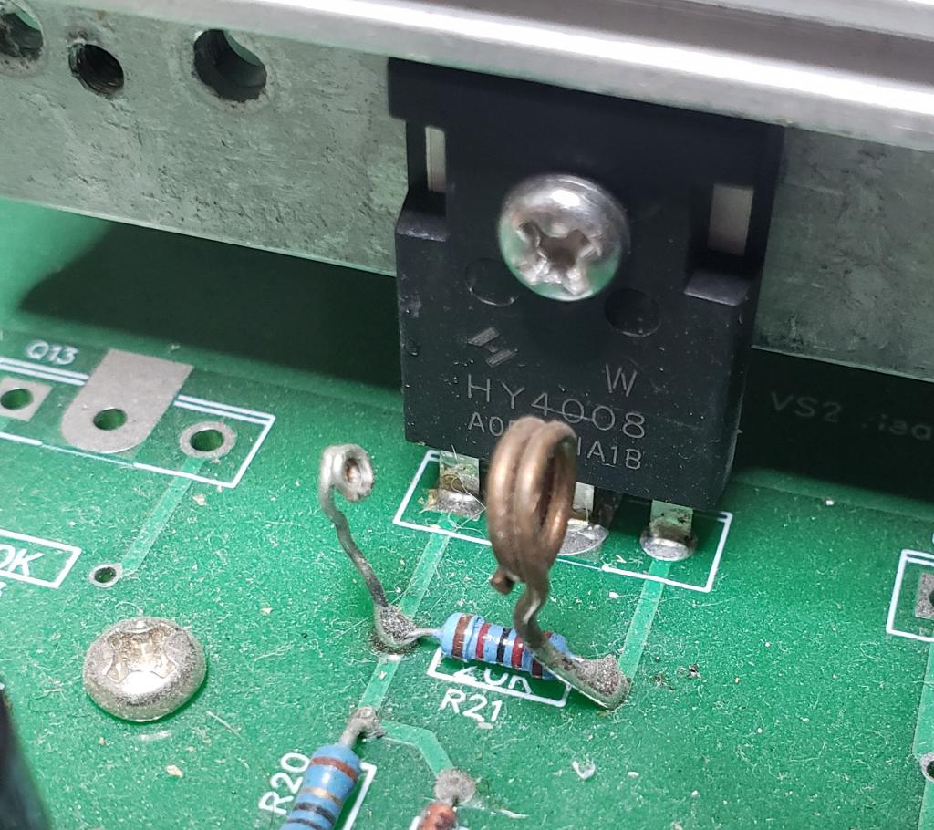
I made a simple 4 mosfet/ no capacitors/ no primary test rig as shown below:
There are no capacitors connected other than what is in the power supply. There is no primary connected either.
Then I connected the probes, yellow trace = HI side gate, green trace = LO side gate with ground to negative power.
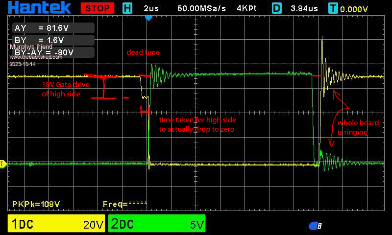
The first pic shows the trace (single shot) with the EG8010 dead time set to 300nS and a 472 capacitor at the input of the FOD3182 driver. Output from that driver goes to a totem pole, its emitters go directly to the gates via a 4R7 resistor.
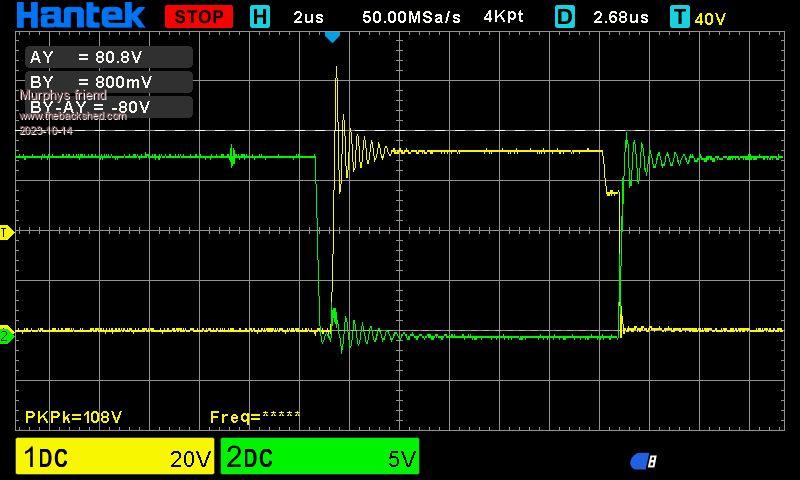
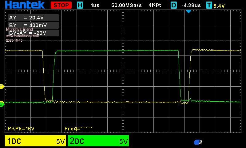
The second pic is the same but with the EG8010 dead time set to 500nS.
I'm interested to know what causes the ringing at the yellow trace, if the dead time is OK and, perhaps, if I'm doing the measurement wrong (DSO's are very new to me )
poida Guru Joined: 02/02/2017 Location: AustraliaPosts: 1480
Posted: 10:50am 14 Oct 2023
Copy link to clipboard
Print this post
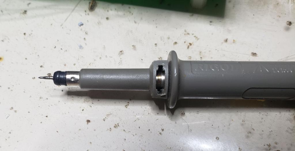
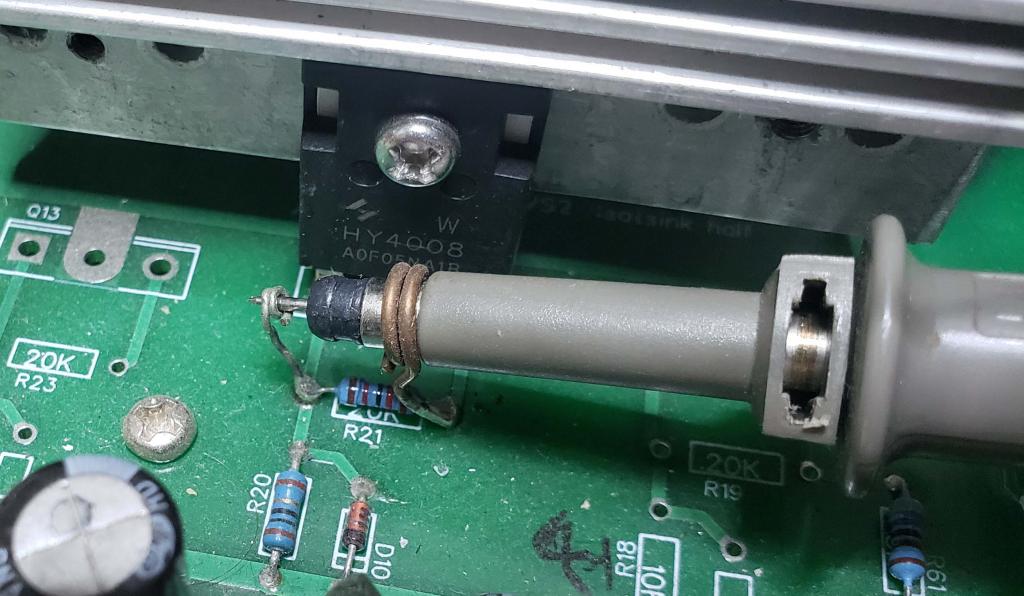
when I am looking at this sort of signal I prefer not to use the ground lead and clip. I remove the tip clip/hood and ground lead
solder on the circuit a place to insert the probe
and then stick the probe in the wire holder
This removes all extra signal errors (including ringing) from the probe's ground lead and clip.
Any ringing now seen is due to the signal present at the probe tip.
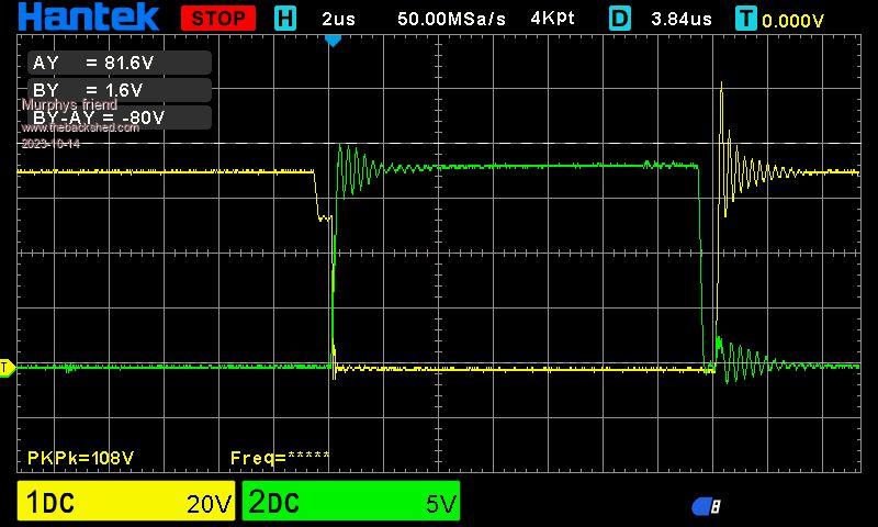
Looking at the above DSO captures I suspect it's not ALL due to the ground lead. I think there is a long ground return path in your test inverter. (edit: no. not this) Something is not quite right.
Maybe try looking at one of the 4 outputs from the 8010 using the very short probe wire setup and see if you get a nice not ringing square wave. You might find that you get clean signals when the 8010 is not connected to the inverter. This will mean the signal is degraded somewhere on the inverter board.
The config of the DSO seems about right. 50 M samples /second and 2 uSec /division is good for this sort of work with 20kHz PWM There will be 100 samples of the signal for each horizontal division and that is plenty.
Can I suggest you first get good looking traces from the low side drive alone. And using the probe tip mounting as I use. This will show exactly what the FET Gate is doing, relative to it's Source pin. Then once that is sorted out and you are fine, then add the high side.
I can send to you the Pirtek isolated probe of mine to play with if you like. It will float on the 100V high side and show again what the voltage of the Gate is doing relative to the (high side) Source.
This is a good trace to look at. We can compare this with maybe one with 1uS dead time and see the differences.
This is what I see:
Edited 2023-10-14 20:54 by poidawronger than a phone book full of wrong phone numbers
poida Guru Joined: 02/02/2017 Location: AustraliaPosts: 1480
Posted: 11:02am 14 Oct 2023
Copy link to clipboard
Print this post
Also, have a play with the vertical position controls, to offset down channel 1 so that the narrow step lines up with channel 2's zero position. And increase ch1 gain to 5V. This will then have ch1 (Yellow) showing the same amplitude as ch2 (Green). The ringing on ch1 will be huge though. I think the primary winding/choke/toroid is wanting to oscillate. Or maybe the totem pole drive is doing it. Or something else.. We will find out what it is.
I think you need more dead time. This will kill the ringing and not cost too much in wasted power.wronger than a phone book full of wrong phone numbers
Murphy's friend Guru Joined: 04/10/2019 Location: AustraliaPosts: 678
Posted: 03:16pm 14 Oct 2023
Copy link to clipboard
Print this post
Thanks Poida, I'll work through your suggestions.
As mentioned, this was just on a small test board rig, not the real inverter with caps & toroid or choke. I basically need to learn how to drive that DSO and your probe suggestions are very helpful.
I'm also experimenting with a different approach to obtain the isolated gate drive. First the 50+ supply is dropped to 12V, non isolated. This then feeds 4 isolated 12 to 15V boost converters, rated 2W each. These are much easier to find than small isolated 50+V to 15V buck converters.
Murphy's friend Guru Joined: 04/10/2019 Location: AustraliaPosts: 678
Posted: 07:42am 15 Oct 2023
Copy link to clipboard
Print this post
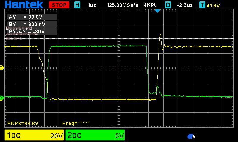
I tried that improved probe technique, much improved traces.
The pic below shows the Hi and LO gate drive only, no power to the mosfets. There seems to be plenty of dead time and no ringing, so problem is at the mosfets switching.
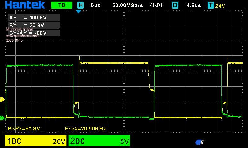
For the next pic I applied power to the mosfets, connected a small load (10W) and fitted a ferrite bead at each drain leg. This seems to reduce the ringing a fair bit.
The last pic is with a fixed frequency drive (EG8010 disabled), 10W load and drain ferrite bead.
Any comments are welcome.
Solar Mike Guru Joined: 08/02/2015 Location: New ZealandPosts: 1228
Posted: 01:23am 16 Oct 2023
Copy link to clipboard
Print this post
There seems to be something wrong with the yellow channel trace when loaded, its a little slow to turn on and even slower to turn off compared to the green, resulting in some overlap which is not good. Not sure what your driver stage is or how many paralleled mosfets are in circuit.
I would test it with just a single device in each leg, remove the ferrite beads, and decrease the gate resistor to something like 1.5R. Once that is looking ok, then add the addition mosfets by putting their gate resistors back in and re-check. Only in unusual circumstances should the beads be required.
Cheers Mike
poida Guru Joined: 02/02/2017 Location: AustraliaPosts: 1480
Posted: 06:41am 16 Oct 2023
Copy link to clipboard
Print this post
wow, that is such an improvement in signal quality
Looking at the latest ones, I still would suggest more dead time. Increase it enough such that there is a clear gap in time between high->low and low->high
We might be thinking that this is what the output voltage will be doing but the FETs are not instantaneous. They have a delay for their output from the Gate drive.
But surely you must be enjoying seeing what the hell is going on here...
The behavior of the FET is a bit of a story At time 0.0 seconds we pull the Gate from 0.0V (relative to Source) to 15V. Some time later the FET starts to change and bring the Drain down to the Source voltage. This is not a simple instant step change. First the Gate charges up (it has a known and significant capacitance) Then the Source/Drain resistance drops. Gradually. Then finally the Gate is at 15V and the FET is at Rds(on) Now it does not change anything until we pull the Gate back down to Source voltage.
We need to give them time to do their stuff.wronger than a phone book full of wrong phone numbers
Murphy's friend Guru Joined: 04/10/2019 Location: AustraliaPosts: 678
Posted: 09:47am 16 Oct 2023
Copy link to clipboard
Print this post
Thanks Poida, you are right it's great fun to actually see what's going on. Should have bought that DSO years ago...
I'll mess around a bit more with dead time adjustments before sticking the DSO probes into my spare inverter, not the rickety test set up I described above. Should be interesting to see.
Murphy's friend Guru Joined: 04/10/2019 Location: AustraliaPosts: 678
Posted: 06:39am 22 Oct 2023
Copy link to clipboard
Print this post
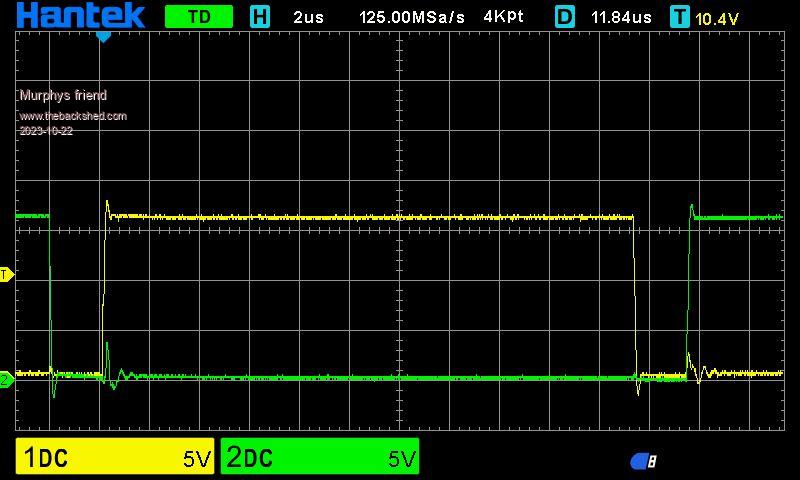
Following Poida's advise I set a long dead time (5.6nF caps) and put both probes to the LO side gates.
This is what shows there:
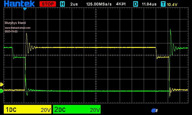
Then I placed both probes at the HI side gates:
I'm curious to know what I can do to make the mosfet turn off time faster at the HI side gates so they do not overlap the turn on of the LO side gate. Setting different dead times appears to only affect the width of the step at initial turn off.
Solar Mike Guru Joined: 08/02/2015 Location: New ZealandPosts: 1228
Posted: 07:13am 22 Oct 2023
Copy link to clipboard
Print this post
Perhaps swap the High side FOD3182 drivers with the Lo-side ones, if you have them in sockets, to make sure they are not the problem. What transistors are you using for the Totem pole buffers, its almost as if they are not being driven hard enough (or faulty) to quickly charge\discharge the Hi-side mosfet gates; or the Hi side driver Vee supply capacitance is too small.
In the past I have had problems with the FOD3182's (from AliExpress) and thrown them in the bin, no longer use them.
Cheers Mike
wiseguy Guru Joined: 21/06/2018 Location: AustraliaPosts: 1297
Posted: 09:34am 22 Oct 2023
Copy link to clipboard
Print this post
In my opinion, the high side gates are turning off just fine, the first step down on the green trace and the plateau under it is the gate being off. After the delay time as per the lower FETs dead time (~ 2uS), when the lower FETs turn on and pulls the floating toroid winding low, the upper FET had been off already for ~ 2uS. ie you don't have a problem - if it ain't broke don't fix it.
To see what is really happening you need an isolated differential probe and then you can place the ground for the second trace at the source of the upper FET, don't try to connect the ground trace of your current setup to the upper source and gate unless you are just observing one trace/one channel and either the 240V CRO is isolated or the Inverter is totally floating relative to ground.
What you are currently looking at is the upper gate drive relative to battery ground and when the upper FET turns on you have battery voltage with the gate drive signal riding on top so the total voltage the probe sees will be battery+ voltage plus the gate drive voltage - you can see at the highest point (green trace) the voltage is ~ 75V, the first plateau of the green trace is the same as what the source is ie battery voltage (~ 60V) without the gate drive added to it. The reason the first plateau is at ~ 60V is that when the upper FET turned off the upper gate voltage became the same as the upper source which, because it was pulled up to battery voltage during the on time it stays floating at batt+ voltage until the lower FET pulls it to ground after the dead time, simple huh ?
It may hurt your head a bit to get around this but persevere. Edited 2023-10-22 19:44 by wiseguyIf at first you dont succeed, I suggest you avoid sky diving.... Cheers Mike
Murphy's friend Guru Joined: 04/10/2019 Location: AustraliaPosts: 678
Posted: 10:23am 22 Oct 2023
Copy link to clipboard
Print this post
Thanks Solar Mile and Wiseguy Mike.
I'll try that FOD3182 swap, they are in sockets.
As mentioned before, this is a mock up test inverter with no transformer connected. Its fully floating, the DC power comes from the bench supply.
Wiseguy, thanks for explaining where the 75V come from, I was wondering as the supply is only set to 56V or so. Now my head is spinning trying to grasp how it all works .
But, as you say its working and don't need fixing. Its just that I thought that the upper and lower gate traces should look similar, just different voltages.
I won't bother with isolated differential probes yet, still trying to get the hang of the many features this DSO has
wiseguy Guru Joined: 21/06/2018 Location: AustraliaPosts: 1297
Posted: 11:00am 22 Oct 2023
Copy link to clipboard
Print this post
If you compare them, the first plateau of the green is identical in width to the lower FETs gate drive trace. So how do you make correct more correct? When the lower FETs turn on their source and drain are at the same potential - ground and the gate is 15V higher than ground. When the upper FETs turn on their drain and source are at the same potential VBatt, but the gate that is turning them on is ~15V higher than the source and drain (VBatt + 15).
I personally would be happy with ~ 250nSec of dead time or to be really conservative 500nSecs. You currently have about 2000 Nano secs. I looked at the idle current for the setting of dead time with most of the bulk capacitor removed (just a couple of uF as temporary) and then reduce dead time until you see the current begin to increase and then just double the dead time for a reasonable safety margin.
I predict that swapping any/all FOD3182s will make no discernible difference.If at first you dont succeed, I suggest you avoid sky diving.... Cheers Mike
Murphy's friend Guru Joined: 04/10/2019 Location: AustraliaPosts: 678
Posted: 03:11pm 22 Oct 2023
Copy link to clipboard
Print this post
Thanks Mike, your reply helps me a lot in understanding more about mosfets - they were not yet invented back then when I did my training in electrical/ electronics.
I appreciate your dead time suggestions and will incorporate them in the inverter I'm re building. Good tip about selecting a suitable dead time, thanks.
The 2000nS was chosen to clearly see what happens at the switch over.
Another question; The oscillation seen on the upper part of the traces are a lot worse if I remove the two ferrite beads I put on the drain pin of each mosfet. Any other suggestion what I could try to minimise them?
poida Guru Joined: 02/02/2017 Location: AustraliaPosts: 1480
Posted: 10:26pm 22 Oct 2023
Copy link to clipboard
Print this post
that oscillation looks a lot like what I saw when I was debugging the single board inverter yesterday. I had more than that due to not having any capacitor fitted to the DC supply.
It was removed completely when I fitted the 10,000uF capacitor once all issues were sorted out. So I am wondering if you have enough caps fitted to this test unit.wronger than a phone book full of wrong phone numbers
wiseguy Guru Joined: 21/06/2018 Location: AustraliaPosts: 1297
Posted: 11:26pm 22 Oct 2023
Copy link to clipboard
Print this post
Depending on layout trace lengths etc if you place a capacitor, ceramic is usually best or polyester/film also good of about 100n physically close to the non FET side of the bead (Batt+/bead junction) to the source of the low side FET, keeping the capacitor wires as short as practicable, the ringing being reflected back to the gate from the drain should be at its lowest value. If ringing is still present on the gate then it might also be due to the gate drive/physical layout of the gate drive.
In the circuit you are experimenting with is there just an upper and lower FET ie 4 in total for the H bridge? Also in the above 2 pictures is the node of the lower drain and upper source actually connected to a load ?
Going back to the last picture in the previous 3 posted by you I see nothing wrong with any of the traces. The green trace is low for most of the trace whilst the upper trace yellow is high (and upper FET on). But at the end of the yellow trace when it turns off the green trace dips below ground that is what I usually see when energy from inductance of the load freewheels through the lower FETs body diode and why there is a slight dip negative at the end of the green trace (the diode drop of the internal body diode).
The body diode dip can also occur just from energy coupled to the lower drain from the upper FET turning off and the upper FETs source steps down to a much lower level from VBatt causing current flow through the lower body diode.
That dip is also an indication of the true dead time which can be seen as ~ 2 divisions of 5 for a 5uSec per division sweep speed or ~ 2uS.If at first you dont succeed, I suggest you avoid sky diving.... Cheers Mike
Murphy's friend Guru Joined: 04/10/2019 Location: AustraliaPosts: 678
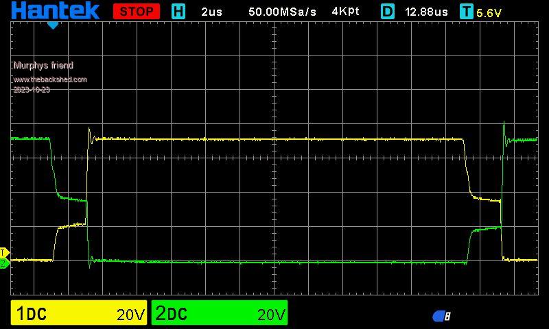
Posted: 08:34am 23 Oct 2023
Copy link to clipboard
Print this post
Thanks wiseguy, yes, just 4 fets and no load.
Today I have answered my question above when applying a load - the ringing disappeared. I also added a 10,000uF cap (had none before) but it was on longish leads. It still helped a bit. This is the screenshot today:
I will experiment with the small cap addition you suggest when I get the PCB I ordered. All the above was with an experimental mosfet power board, to find out what to look for when I put the small caravan inverter together. When this is finished (and working ) I'll continue with the inverter downsizing thread I started earlier.
Thank you for all the wise input, much appreciated.
wiseguy Guru Joined: 21/06/2018 Location: AustraliaPosts: 1297
Posted: 03:02pm 23 Oct 2023
Copy link to clipboard
Print this post
Nice clean waveform, very symmetrical, isn't it nice to have a decent CRO and have a whole new world open up to you ? That dead time is nearly 10% of your possible drive waveform period, its main negative effect is to drop out of regulating the output voltage a bit earlier ie it stops regulating at 46V instead of 44V.
I think your waveforms look really good now. I quite like ferrite beads despite some others having an aversion to them ! If there is minimal to no ringing then leave them off but if there is ringing that seems to resist all attempts to suppress it without success then try a ferrite bead.If at first you dont succeed, I suggest you avoid sky diving.... Cheers Mike
Murphy's friend Guru Joined: 04/10/2019 Location: AustraliaPosts: 678
Posted: 08:24am 24 Oct 2023
Copy link to clipboard
Print this post
Thanks Mike, Yes, I will shorten that dead time. I just wanted to see what happens if I make it really long. Thanks for the regulation tip, something else that did not occur to me. I feel like an old dog being taught new tricks , as they say, one never should stop learning.


 )
) 
 .
.
 , as they say, one never should stop learning.