
|
|
Forum Index : Microcontroller and PC projects : Armmite L4: 48-pin support
| Page 1 of 2 |
|||||
| Author | Message | ||||
| matherp Guru Joined: 11/12/2012 Location: United KingdomPosts: 11515 |
Please find attached version 5.05.01 which supports both 32-pin and 48-pin parts. 2018-11-30_230951_ArmmiteL4.zip This is tested on a STM32L433CCT6 but will also run on STM32L431CCT6. The chip is mounted on an Adafruit 48-pin LQFP adapter . The chips are 0.5mm pitch so pretty easy to solder. I haven't tested all pin functionality but all MMBasic functionality works fine as does the SPI flash file system. 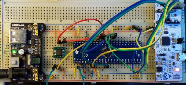 Pinout for the 48-pin chips is: { NULL, 0, PUNUSED , NULL, 0,""}, // pin 1 VBAT { GPIOC, GPIO_PIN_13, DIGITAL_IN | DIGITAL_OUT, NULL, 0, "C13"}, // pin 2 { NULL, 0, PUNUSED , NULL, 0,""}, // pin 3 OSC32_IN { NULL, 0, PUNUSED , NULL, 0,""}, // pin 4 OSC32_OUT { NULL, 0, PUNUSED , NULL, 0,""}, // pin 5 PH0 { NULL, 0, PUNUSED , NULL, 0,""}, // pin 6 PH1 { NULL, 0, PUNUSED , NULL, 0,""}, // pin 7 NRST { NULL, 0, PUNUSED , NULL, 0,""}, // pin 8 VSSA { NULL, 0, PUNUSED , NULL, 0,""}, // pin 9 VDDA { GPIOA, GPIO_PIN_0, DIGITAL_IN | DIGITAL_OUT | ANALOG_IN , ADC1, ADC_CHANNEL_5,"A0"}, // pin 10 { GPIOA, GPIO_PIN_1, DIGITAL_IN | DIGITAL_OUT | ANALOG_IN , ADC1, ADC_CHANNEL_6,"A1"}, // pin 11 SPI-CLK { NULL, 0, PUNUSED , NULL, 0,""}, // pin 12 CONSOLE-TX { GPIOA, GPIO_PIN_3, DIGITAL_IN | DIGITAL_OUT | ANALOG_IN , ADC1, ADC_CHANNEL_8,"A3"}, // pin 13 { GPIOA, GPIO_PIN_4, DIGITAL_IN | DIGITAL_OUT | ANALOG_IN , ADC1, ADC_CHANNEL_9,"A4"}, // pin 14 DAC-1 { GPIOA, GPIO_PIN_5, DIGITAL_IN | DIGITAL_OUT | ANALOG_IN , ADC1, ADC_CHANNEL_10,"A5"}, // pin 15 DAC-2 { GPIOA, GPIO_PIN_6, DIGITAL_IN | DIGITAL_OUT | ANALOG_IN , ADC1, ADC_CHANNEL_11,"A6"}, // pin 16 SPI-IN { GPIOA, GPIO_PIN_7, DIGITAL_IN | DIGITAL_OUT | ANALOG_IN , ADC1, ADC_CHANNEL_12,"A7"}, // pin 17 SPI-OUT { GPIOB, GPIO_PIN_0, DIGITAL_IN | DIGITAL_OUT | ANALOG_IN , ADC1, ADC_CHANNEL_15,"B0"}, // pin 18 { GPIOB, GPIO_PIN_1, DIGITAL_IN | DIGITAL_OUT | ANALOG_IN , ADC1, ADC_CHANNEL_16,"B1"}, // pin 19 COUNT { GPIOB, GPIO_PIN_2, DIGITAL_IN | DIGITAL_OUT , NULL, 0,"B2"}, // pin 20 { GPIOB, GPIO_PIN_10, DIGITAL_IN | DIGITAL_OUT , NULL, 0,"B10"}, // pin 21 COM2-TX { GPIOB, GPIO_PIN_11, DIGITAL_IN | DIGITAL_OUT , NULL, 0,"B11"}, // pin 22 COM2-RX { NULL, 0, PUNUSED , NULL, 0,""}, // pin 23 VSS { NULL, 0, PUNUSED , NULL, 0,""}, // pin 24 VDD { GPIOB, GPIO_PIN_12, DIGITAL_IN | DIGITAL_OUT , NULL, 0,"B12"}, // pin 25 { GPIOB, GPIO_PIN_13, DIGITAL_IN | DIGITAL_OUT , NULL, 0,"B13"}, // pin 26 { GPIOB, GPIO_PIN_14, DIGITAL_IN | DIGITAL_OUT , NULL, 0,"B14"}, // pin 27 { GPIOB, GPIO_PIN_15, DIGITAL_IN | DIGITAL_OUT , NULL, 0,"B15"}, // pin 28 { GPIOA, GPIO_PIN_8, DIGITAL_IN | DIGITAL_OUT , NULL, 0,"A8"}, // pin 29 { GPIOA, GPIO_PIN_9, DIGITAL_IN | DIGITAL_OUT , NULL, 0,"A9"}, // pin 30 COM1-TX { GPIOA, GPIO_PIN_10, DIGITAL_IN | DIGITAL_OUT , NULL, 0,"A10"}, // pin 31 COM2-RX { GPIOA, GPIO_PIN_11, DIGITAL_IN | DIGITAL_OUT , NULL, 0,"A11"}, // pin 32 { GPIOA, GPIO_PIN_12, DIGITAL_IN | DIGITAL_OUT , NULL, 0,"A12"}, // pin 33 COM1-DE { NULL, 0, PUNUSED , NULL, 0,""}, // pin 34 SWDIO { NULL, 0, PUNUSED , NULL, 0,""}, // pin 35 VSS { NULL, 0, PUNUSED , NULL, 0,""}, // pin 36 VDD // { NULL, 0, PUNUSED , NULL, 0,""}, // pin 37 SWCLK { NULL, 0, PUNUSED , NULL, 0,""}, // pin 38 CONSOLE-RX { GPIOB, GPIO_PIN_3, DIGITAL_IN | DIGITAL_OUT , NULL, 0,"B3"}, // pin 39 SPI2-CLK { GPIOB, GPIO_PIN_4, DIGITAL_IN | DIGITAL_OUT , NULL, 0,"B4"}, // pin 40 SPI2-IN { GPIOB, GPIO_PIN_5, DIGITAL_IN | DIGITAL_OUT , NULL, 0,"B5"}, // pin 41 SPI2-OUT { GPIOB, GPIO_PIN_6, DIGITAL_IN | DIGITAL_OUT , NULL, 0,"B6"}, // pin 42 I2C-SCL { GPIOB, GPIO_PIN_7, DIGITAL_IN | DIGITAL_OUT , NULL, 0,"B7"}, // pin 43 I2C-SDA { NULL, 0, PUNUSED , NULL, 0,""}, // pin 44 BOOT0 { GPIOB, GPIO_PIN_8, DIGITAL_IN | DIGITAL_OUT , NULL, 0,"B8"}, // pin 45 { GPIOB, GPIO_PIN_9, DIGITAL_IN | DIGITAL_OUT , NULL, 0,"B9"}, // pin 46 { NULL, 0, PUNUSED , NULL, 0,""}, // pin 47 VSS { NULL, 0, PUNUSED , NULL, 0,""}, // pin 48 VDD |
||||
| sagt3k Guru Joined: 01/02/2015 Location: ItalyPosts: 313 |
Hi matherp Very good. Is it possibile to have USB as console on PA11/PA12  ? ?Antonio |
||||
| matherp Guru Joined: 11/12/2012 Location: United KingdomPosts: 11515 |
No - not enough flash and I HATE usb consoles. They just create problems with embedded applications, particularly during development when frequent restarts are needed |
||||
| sagt3k Guru Joined: 01/02/2015 Location: ItalyPosts: 313 |
OK matherp I did not know about these problems, so perfect like that.  When you have free time ..., do You have a simple schematic of how you are using this micro? Thanks Antonio |
||||
| sagt3k Guru Joined: 01/02/2015 Location: ItalyPosts: 313 |
Hi matherp Is there possibility to have software COM2 on L4-32pin? Thanks Antonio |
||||
| matherp Guru Joined: 11/12/2012 Location: United KingdomPosts: 11515 |
Not in the near future but I'll put it on the list to look at |
||||
| sagt3k Guru Joined: 01/02/2015 Location: ItalyPosts: 313 |
Hi matherp I'm trying to work your firmware with a my old PCB for stm32l4x 48pin and STM32L431. I have all the fundamentals pins connected with caps, res and crystal. If try my simple firmware ports, uart, timer the micro works. But If I try to put your firmware the micro seems blocked. Apart boot0, nrst, do I need to take some precautions? Thanks Antonio |
||||
| matherp Guru Joined: 11/12/2012 Location: United KingdomPosts: 11515 |
From the manual which is nearing completion finally. The other thing worth trying is to disconnect the ST-LINK to make sure it isn't holding NRST. Is your chip definitely a CC and not a CB? The CB is only 128K flash. The firmware would probably load but can't run. Latest firmware (checked on a stm32l433cct6) attached 2019-03-19_232030_ArmmiteL4.zip |
||||
| sagt3k Guru Joined: 01/02/2015 Location: ItalyPosts: 313 |
Thanks. I have only STM32L431CCT6.is it ok with your firmware? |
||||
| matherp Guru Joined: 11/12/2012 Location: United KingdomPosts: 11515 |
Yes definitely. The reason I raise the CB/CC issue is that I bought CC of RS and they shipped CB which I only noticed when the firmware wouldn't run. |
||||
| grumpyoldgeek Regular Member Joined: 30/07/2018 Location: United StatesPosts: 53 |
Matherp, Using the above design with the 32khz crystal, can the firmware be loaded through the serial port if BOOT0 is pulled up? |
||||
| matherp Guru Joined: 11/12/2012 Location: United KingdomPosts: 11515 |
Yes: no problem |
||||
| grumpyoldgeek Regular Member Joined: 30/07/2018 Location: United StatesPosts: 53 |
Thanks. I've been trying to build a prototype similar to what you've done, but I don't see a waveform on the crystal terminals. I've double checked the wiring and tried 2 crystals and a ceramic resonator and I still get nothing. I'll try a new cpu next. |
||||
goc30 Guru Joined: 12/04/2017 Location: FrancePosts: 435 |
Hi Peter question: is-it possible to know speed of L4 as print CPU 'question > CPU speed : 80 'response |
||||
| grumpyoldgeek Regular Member Joined: 30/07/2018 Location: United StatesPosts: 53 |
Peter, The ARMmite L4 manual says to ground pin 3 of the W25Q128JV flash memory chip. The datasheet for the part shows pin 3 grounded to write protect the part. Is this an error, or are you using a register inside the part to enable writes? I also noticed in the STM32L433 datasheet that the NRST pin has an internal weak pullup, so a 10k pullup is probably unnecessary if the pin is not used otherwise. I have everything working except the flash memory, which I have not connected yet. I spent a lot of time thinking my prototype was not working because I could not see any signals on the oscillator pins. It turns out that the unprogrammed part uses the internal oscillator and there is no signals on the pins until code turns on the oscillator. |
||||
| matherp Guru Joined: 11/12/2012 Location: United KingdomPosts: 11515 |
From the W25Q128JV datasheet SRP and SRL are zero so "/WP pin has no control. The Status register can be written to after a Write Enable instruction, WEL=1. [Factory Default] " I think I just tied WP low for something to do with it but it could equally be high, just best practice not to leave it floating. |
||||
| grumpyoldgeek Regular Member Joined: 30/07/2018 Location: United StatesPosts: 53 |
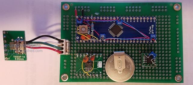 Prototype is fully functional. A couple of notes, pin 2 on the L433 does not work for flash chip select, I ended up using pin 5. 32khz crystal is only active after loading firmware. When active, you should see a rough sine wave on pins 3 & 4 of about 120 millivolts. DO NOT waste your time trying to get the STM Serial Loader Demo to work, use the STMCube Programmer as the documentation says. It works great. Schematics will follow in a few days. |
||||
| grumpyoldgeek Regular Member Joined: 30/07/2018 Location: United StatesPosts: 53 |
I'm seeing a VBAT current draw of about 60 microamperes when VDD is removed. Is that normal? I need something closer to 2-3 microamperes for a coin cell. |
||||
| matherp Guru Joined: 11/12/2012 Location: United KingdomPosts: 11515 |
No, should be approx 0.4uA |
||||
| grumpyoldgeek Regular Member Joined: 30/07/2018 Location: United StatesPosts: 53 |
Peter, I'm still having problems with VBAT current consumption. I've loaded firmware 2019-03019 and the processor behaves correctly in all other respects. I removed all components from the processor to insure that there are no sneak paths for parasitic current draw. All that is connected to it is the 32Khz crystal and its capacitors and a high quality meter capable of measuring tenths of micro-amperes which is in series with the coin cell and the VBAT pin. The circuit board has been meticulously cleaned. I connect a coin cell to VBAT and apply 3.3 volts to Vdd. The processor works fine and the 32Khz oscillator is running. VBAT current is zero. I remove the 3.3 volts and VBAT current is 0.3 micro-amperes. The oscillator is running. I reapply 3.3 volts and then remove it. VBAT current goes up to 60 micro-amperes. Subsequent cycling of Vdd does not improve things. Neither does resetting by momentarily grounding NRST. The only way to get VBAT back to 0.3 micro-amperes is to remove both VBAT and Vdd and reapply them. Any help you can give would be appreciated. I'd be happy to replace the processor chip if you think that might help. |
||||
| Page 1 of 2 |
|||||
| The Back Shed's forum code is written, and hosted, in Australia. | © JAQ Software 2026 |
