
|
|
Forum Index : Microcontroller and PC projects : 8, 14 & 18 pin DIL versions of 170 uM...
| Page 1 of 4 |
|||||
| Author | Message | ||||
Grogster Admin Group Joined: 31/12/2012 Location: New ZealandPosts: 9975 |
Hi-de-hi. 
As hinted by another member here who would like uM chips in smaller DIL packages, I have bought some QFN chips from Microchip Direct, with which I intend to design some 8-pin, 14-pin and 18-pin versions of the 28-pin uM. The only thing that will change with the smaller versions, is your not being able to access the higher pin numbers. At this stage, PCB's will be standard skinny DIL footprint, with the QFN fitted. The QFN is a fun chip - 6mm square with 0.65mm pin spacing. I don't expect this to be too much of a problem though, as I have a reflow workstation(a Hako one), and am also planning to build a reflow oven too. This will give me a chance to play with reflow soldering, and with the chips only being $3 or so each, it does not really matter if I kill one or two, while perfecting my reflow technique. 
I'll keep you all posted. Assuming they would be wanted by anyone other then the member who has brought this idea to my attention, then I would release the Gerbers so others can make their own. The module will be minimalistic - just the chip and the DIL footprint. I MIGHT add the 10uF cap to VCAP, IF there is enough room, but skinny DIL is not much space to work from! EDIT: Even with QFN, it is gonna be near-on impossible to get the QFN footprint inside a skinny DIL footprint, so I am probably going to have 1.5x DIL(10mm) - still on 2.54 grid, but one-and-a-half times skinny width - still pretty small, and still easy enough to fit on PCB's, and is still breadboard compatible. Smoke makes things work. When the smoke gets out, it stops! |
||||
| hitsware Guru Joined: 23/11/2012 Location: United StatesPosts: 535 |
> 10uF cap to VCAP I forget the function of that cap ? AND That's another pin consideration . I assume it's for some referance voltage and may not be appropos for most routines. Maybe for the ADC's ? |
||||
| Grogster Admin Group Joined: 31/12/2012 Location: New ZealandPosts: 9975 |
I have the basic PCB designed - I wll upload image later. Vcap is on-board, which allows use of another I/O pin. Having just thinking I had perfected the design, I discover in the datasheet that the QFN part has different pin-assignments. Example: Vcap is pin 20 on the DIL package, but it is pin 17 on the QFN. MCLR is pin 1 on the DIL, but it is pin 26 on the QFN.... Just as well I noticed that one!
EDIT: I plan to do a couple of versions of the 8-pin one, so that you can have a standard one, or one that has the COM ports, and maybe a third one that has SPI and I2C. ...just thinking about that at this stage, as in some ways, doing that would be re-inventing the wheel, so to speak. Smoke makes things work. When the smoke gets out, it stops! |
||||
bigmik Guru Joined: 20/06/2011 Location: AustraliaPosts: 2981 |
Hi Grogs, Can you upload a layout so that I can offer an opinion (not that my I think my opinion means more than yours or others). Maybe you can put some small config links to say have I2C lines there or Analog ones etc.. I think I2C would be a great addition. even some solder pads to connect wires to. Regards, Mick Mick's uMite Stuff can be found >>> HERE (Kindly hosted by Dontronics) <<< |
||||
| hitsware Guru Joined: 23/11/2012 Location: United StatesPosts: 535 |
I say : for 8 pin DIP : ........................ pin 1 ... Vcc ............... pin 8 ... 0V pin 2 ... serial in ......... pin 7 ... serial out pin 3 ... pwm 1-A ........... pin 6 ... pwm 2-A pin 4 ... pwm 1-B ........... pin 5 ... pwm 2-B Note: the pwm pins are not restricted to pwm |
||||
| Grogster Admin Group Joined: 31/12/2012 Location: New ZealandPosts: 9975 |
The original concept was uM pins 4,5,11,12 and 21 - but that was before I discovered the QFN had a different pinout! 
That is still kinda the plan - depends on how much space I have to route tracks. @ hitsware - I need to reserve 2 pins for PGD and PGC, otherwise, there will be no way to program the device with the uM firmware.
Having said that, my pins list above does cater for at least one PWM output. If that is not enough, then the pending 14's and 18's would. EDIT: Opps - PWM 1A and 1B ARE pins 4 & 5 - sorry, hitsware! 
[Quote=Mick]Can you upload a layout so that I can offer an opinion Will do. Smoke makes things work. When the smoke gets out, it stops! |
||||
| bigmik Guru Joined: 20/06/2011 Location: AustraliaPosts: 2981 |
Hi Grogs, Just a bit of food for thought... 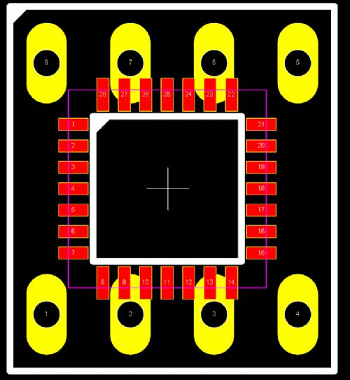
Here is an accurate layout of the QFN over an 8pin socket.. The purple square is the physical size of the chip. It obviously wont fit as shown BUT If you were to use surface mount pins (mounted on the bottom) and not through hole then the QFN mounted on the top and you should have some room for a `couple' of solder link options to enable the same PCB to have 2 or more different pin configurations. All that in a small standard 8pin IC package. Regards, Mick Mick's uMite Stuff can be found >>> HERE (Kindly hosted by Dontronics) <<< |
||||
| viscomjim Guru Joined: 08/01/2014 Location: United StatesPosts: 925 |
kind of like a basic stamp but soooo much better!!!! I want! |
||||
| Grogster Admin Group Joined: 31/12/2012 Location: New ZealandPosts: 9975 |
@ Mick - My CAD does not like that idea much - it WILL overlap - even at pin level. 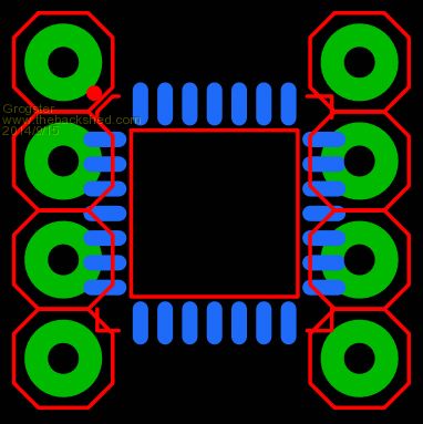
Then there are two caps and a resistor yet to fit... I suspect it is probably a little close? I do see what you are getting at though with the DIL pins on the bottom copper only - you could put the pin through, solder it on the bottom, and trim it off at the top. My only concern is lack of space - it is really pushing it!
Where would I get serface-mount pins from? Do you happen to have a part in mind you could point me to? EDIT: I suppose I don't NEED to have a 100n cap on the power pins, and I don't NEED to have a 10k pull-up on MCLR on the board - they could be external. I could just put Vcap on the board, not the other two. That might free up some room for config pads you mention.... Smoke makes things work. When the smoke gets out, it stops! |
||||
| bigmik Guru Joined: 20/06/2011 Location: AustraliaPosts: 2981 |
Hi Grogs, Yours is showing the same as mine.. they `just' miss the pins (you probably have slightly larger holes in your part but even your picture shows them missing on the LHS) but if you use surface mount pins then they wont protrude at all into the top layer just use vias to drop the signals down from top to bottom. Tight.. YES!! Impossible .. NO!! I see that you could have a SMD cap and 0805 resistors still. Of course you dont need to suit an 8 pin socket it can be a SMD 8pin 2x4 pin header strip mounted on the bottom that gives more room underneath for solder config pads.. You could also have 2 pads on the top for I2C if you cant/dont wish to route them to config lines. If we can come up with a pin-pin mapping with any options and `support' components it will be easier to see if/how it will layout.. but using the SMT parts it would definitely fit a 12pin or 16pin socket. Mind you it would be a bit of a b|tch to hand solder. Mick Mick's uMite Stuff can be found >>> HERE (Kindly hosted by Dontronics) <<< |
||||
| Grogster Admin Group Joined: 31/12/2012 Location: New ZealandPosts: 9975 |
Where can I find SMD pins? Smoke makes things work. When the smoke gets out, it stops! |
||||
| WhiteWizzard Guru Joined: 05/04/2013 Location: United KingdomPosts: 2991 |
Just woke up and seen that my idea from the other thread is already under development
Food for thought - there were two ways that I originally thought to solve the 'limited space' issue: 1> Use surface mount pins (as has also been mentioned by bigmick too). Trouble with these are potential weakness - especially with repeated insertion/removal. But it will result in a small package. 2> Have a vertical mini PCB with right angle pins to form the 'legs'. This can be done but the height of the resultant package would be a little taller than a DIP. Either way, I would jumper the Tx/Rx programming pins (to give 6 I/Os on an 8-pin DIP module ) AND also definitely include vCap onboard (so it is a self contained module). As for which of the 19 I/Os to have as the other six pins (on 8-pin DIP) - there will not be enough room for lots of jumpers so in my eyes the solution is simple - have lots of different PCB versions - one with PWM main functionality, one with I2C main functionality, one with SPI main functionality, etc, etc. WW |
||||
| WhiteWizzard Guru Joined: 05/04/2013 Location: United KingdomPosts: 2991 |
Grogs - I have used these before: |
||||
| WhiteWizzard Guru Joined: 05/04/2013 Location: United KingdomPosts: 2991 |
These staggered pins add strength on longer headers but only 4 pins it is a bit limited. |
||||
| bigmik Guru Joined: 20/06/2011 Location: AustraliaPosts: 2981 |
Grogs, The pins I was referring to are like these but 4 way not 3. These plug into a wiper type IC socket fairly easilly and as you see they are SMT type. Mick 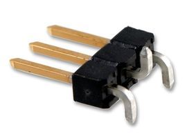
EDIT** I see that this has been answered whilst I was searching for the parts. Mik Mick's uMite Stuff can be found >>> HERE (Kindly hosted by Dontronics) <<< |
||||
| bigmik Guru Joined: 20/06/2011 Location: AustraliaPosts: 2981 |
The Dual type are like these. 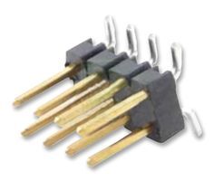
Of course there is no reason the PCB can't be a bit wider by a few mm if you cannot squeeze everything into the space. Mick Mick's uMite Stuff can be found >>> HERE (Kindly hosted by Dontronics) <<< |
||||
| Grogster Admin Group Joined: 31/12/2012 Location: New ZealandPosts: 9975 |
Yeah, that was my way of thinking too - I said as much a few posts back, but it is all up in the air at the moment.
Perhaps that is actually the best way forward? The only problem with that, is that you end up with several different versions of the main concept, and if someone uses the wrong one.... HOWEVER - you'd have to expect that those using the modules, would know which version they would need.
EDIT: @ Mick and WW - thanks for the photos - I had something totally different in mind, but those photos have clarified that for me - ta. Smoke makes things work. When the smoke gets out, it stops! |
||||
| MicroBlocks Guru Joined: 12/05/2012 Location: ThailandPosts: 2209 |
I made something similar some time ago. Did not finish it as i am still in the market for a reflow oven and the QFN's are a real pain to solder. My wish was to make something as compact as possible, not necessarily in the shape of a dip package. I came up with this: 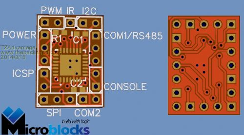
The size is 13.4x18.4 millimeter. 2-Layer, bottom has a GND copper pour. On the left side is reset, power and ICSP in the right order to plug in a pickit. On the right console and Serial/RS485. You could only use those and leave the top and bottom unpopulated depending on your needs. There are only 3 uMite pins unused, ones with the least capabilities. Here is the schematic: 2014-09-15_142142_Schematic_-_MB_uMite_P20.pdf Microblocks. Build with logic. |
||||
| Grogster Admin Group Joined: 31/12/2012 Location: New ZealandPosts: 9975 |
Nice little boards, TZA. Watch the reflow oven thread - I have my oven, I am just waiting on my LCDmite PCB's and LCD's, thermocouples and AD594's to arrive, then I can hook it all up. DIL is PROBABLY still workable - I will wait for more posts from Mick, but I am still kinda liking the 1.5xDIL size(10mm), as it only adds 2.5mm to the width, is still DIL, and is still breadboard friendly. ...several things to think about anyway! Smoke makes things work. When the smoke gets out, it stops! |
||||
| bigmik Guru Joined: 20/06/2011 Location: AustraliaPosts: 2981 |
TZ, Beautiful little boards.. I love them... A question, if I may, the GND `block' that you have in the centre of the PIC, about 4.5mm square, is there a metal tab on the underside of the PIC that mates with this? If so then we cannot run tracks with vias there, which I think would be crucial in fitting it all into a DIL 0.3" layout. Does any one have any suggestions as to which pins would be most desired? I have thoughts of I2C, SPI, Analog, I would like to see if we `CAN' get a one for all PCB laid out in the constraints that a DIP8 would allow. DO we try to keep 5V tolerant lines (none are Analog though)? Keeping with a 0.3" DIP8 socket what is the MAXIMUM PCB size you would like to see? Is 15mm x 15mm too big? Mick EDIT** I am also thinking that the pins could be standard pins but soldered as SMT types.. Especially if the round `samtec' style pins are used.. Mik Mick's uMite Stuff can be found >>> HERE (Kindly hosted by Dontronics) <<< |
||||
| Page 1 of 4 |
|||||
| The Back Shed's forum code is written, and hosted, in Australia. | © JAQ Software 2026 |
