
|
|
Forum Index : Electronics : Wiseguy New Inverter Build Nano R6
| Author | Message | ||||
| nickskethisniks Guru Joined: 17/10/2017 Location: BelgiumPosts: 477 |
Well, I'm close to start building the powerboards soon, but... I will probably use a different mosfet (hy5110) and gateresistor/bead combination. And after reading wiseguys research about the ds beads, I still have some concerns about using the beads. So I'm doing a little bit of research and testing myself and later after populating a powerboard with the same experiments I will share my findings. The matter concerns me after reading some application notes where they point not to use "randomly" beads because they can also worsen things. I know you have several decades of expierence designing power electronics Wiseguy and I trust your gut and research. But It's the part were application notes state to design an application so the mosfet stay out of the avalance region, allthough the energy is very low it can still degrade the mosfet overtime. Personaly I would feel more sure when we can prevent it, you allready hinted (a solution) the use of a 10/15R parallel with the bead, something I didn't understand first when I read about it in an application note. But it is litteraly a resistor soldered on the mosfet leg over the bead. So why not spending the extra effort after spending hours of work taking time to solder those resistors in? Revlac even mentioned it to use some beads in his mppt controller, I hope you probe the mosfet because voltages are higher and the bead might be counter productive. I think the use of a bead will be a good thing, but maybe another bead or some extra measurements to prove it's contribution. So, I allready said I'm doing some testing, well, I tested 4 different beads, with 3 I had about the same results as you. But then the last one, really a tiny bead, this tested wayout better then all the rest. I think the peak halved compared to the other ones, and then with a snubber 1n/10R it was really low compared to the starting point. Tests were done under load ( no transformer or inductor attached) and with load, most of the time a load with high impedance made things better, a low impedance worsened the shoot true during turn off transient. A snubber could greatly reduce the peak of the pulse without load but not so under load. Adding some 100nF close to the mosfets between positive/negative rail helped but not more then a few volts. So, I will devote a new thread on the subject after populating an inverter powerboard. But I think I want to say with my post is that there probably are better suited beads to use, or maybe not. I found out it was in some cases until load was applied... Sorry if I opened a pandora box again.  Here you can see the beads, 3 low are ali express and the one most top is a mouser part, the lowest one performed best in my test setup. 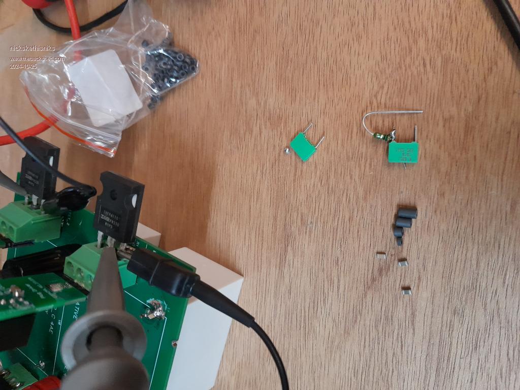 These were the beads: The best one was the only 3.2*1.4*1.2 mm https://nl.aliexpress.com/item/1005004112003854.html?spm=a2g0o.order_detail.order_detail_item.3.35616d762UwNZk&gatewayAdapt=glo2nld Edited 2024-10-25 21:35 by nickskethisniks |
||||
| wiseguy Guru Joined: 21/06/2018 Location: AustraliaPosts: 1296 |
My take on Ferrite bead use and behaviour. The bead placed on the Drain lead of a MOSFET is worthy of a little more discussion and analysis as suggested By Nicks. Ferrite beads were initially created and introduced for a few reasons, most of them associated with higher frequencies. Designers could then exploit their specific behaviours. At HF's they have inherent properties of impedance, inductance, wide band and low loss. My decision to use ferrite beads are mainly due to their high impedance behaviour which usually increases with frequency often up to the GHz region. The inductance and impedance property of a Ferrite bead will reduce with increased DC bias current. At the DC bias current levels in an inverter the bead's inductance will be extremely low during the FET on time and the bead will be fully saturated. For the low inverter switching frequencies from 20 - 50kHz the beads have relatively low internal loss as their saturation is instantaneously reached as the FET turns on, so relative to the total switching period their is minor bead heat produced. It is near impossible for a circuit to have zero inductance at the Drain of the MOSFET, even the Drain leg of the FET introduces inductance, so high speed switching on and especially off is usually accompanied by a decayed "ringing" of the waveform at the Drain of the FET in the MHz range. To reduce the ringing, a bead placed on the Drain lead increases the HF impedance, thereby minimising the circuits Q significantly and the ringing can be reduced to near zero. The main resonance is from the inherent internal capacitance of the FETs Drain and the Drain circuits total inductance. An added benefit of the reduced HF ringing is the reduction of the harmonics and EMI generation from the otherwise very fast switching edges. The other benefit is that when paralleling MOSFETs there can be tendencies for oscillations to occur where paralleled MOSFETs can appear to behave more like a power multivibrator (at very high frequencies in the 10's to 100's of MHz) than the true current sharing that was desired and aimed for by paralleling the MOSFETs. A minor negative side effect of the bead is the energy storage during the FETs on period, this energy discharges during the FETs off time. As there is no current path with the FET now off, the inductor voltage increases until one of two things happen, the FET's Drain avalanches internally and tames the voltage "spike" or the voltage peak is not high enough to avalanche the FET. Due to the high permeability of the "soft" ferrite bead material there is virtually no energy storage of concern and whilst avalanching a MOSFET in a design can be a problematic issue, the very minor energy storage of a small bead can be safely ignored. In my experiments I found that a voltage spike of ~ 20 - 40V could be encountered and simply placing a 4.7 - 12 ohm resistor across either end of the wire passing through the bead could reduce the voltage peak by up to ~ 80% with some minor heating of the resistor. Lastly MOSFETs, since the 80's have focussed on improving the avalanche ratings of available devices. Whilst Trench FETs (most common) are not as good as Planar FETs, their avalanche energy rating is still usually very large. The HY5608 I recommended has a manufacture tested safe maximum avalanche energy rating (not repetitive) of nearly 3 Joules from an inductance of 0.5 millihenries. This is the type of avalanching that really should be avoided. Compare this to the typical ferrite bead inductance of 2uH with very low volumetric storage levels, safe energy dissipation perhaps in the few millijoule range could be expected. To date I have not encountered or been aware of any MOSFET failures through using a ferrite bead placed on the drain, but I am aware of significant levels of EMI interference reduction and visibly very clean switching waveforms. I am hoping that Nicks investigations will also mirror what I found. Edited 2024-10-27 14:09 by wiseguy If at first you dont succeed, I suggest you avoid sky diving.... Cheers Mike |
||||
| KeepIS Guru Joined: 13/10/2014 Location: AustraliaPosts: 2177 |
I also used smaller ferrite beads compared to wiseguys original design, they appear to work as intended but need further testing - just no time the moment. That would be interesting if you get the time, and the only thing I would suggest is changing the probe setup. IMHO you need to remove the probes ground lead and the long nose clamp. Both need to be very short and ground isolated probes (differential probe) with two inputs (even if one probe is the trigger input if its ground lead is connected) Without that, the waveform and amplitudes at these frequencies cannot be fully trusted. I do find the very fast switching of the FETS in this design can cause more RF interference, which I expected and wiseguy also mentioned, a small price to pay for having such low heating of the FETS. EDIT Dam! just posted and then I see wiseguys posted, I haven't read his yet - so disregard if anything contradicts wiseguys post. _ Edited 2024-10-27 14:48 by KeepIS NANO:Inverter V 8.2ks - Linux AvrDude GUI script V4.1 |
||||
| analog8484 Senior Member Joined: 11/11/2021 Location: United StatesPosts: 203 |
Your finding of the smallest bead being more effective (assuming the same material) is consistent with my experience. The bead effectiveness decreases quickly with the gap distance from the pin going through the bead. Also, the Ali beads you used all appear to be Ni-Zn material type which I have found to be less effective than Mn-Zn ones. The Ni-Zn beads are more effective in higher frequency ranges. The Mn-Zn ones are more effective at lower frequency ranges closer to the lower switching frequency range of inverters compared to typical SMPS. Lastly, I have learned to avoid getting beads from Ali as they have inadequate specs and they can differ significantly from one purchase to the next. |
||||
| nickskethisniks Guru Joined: 17/10/2017 Location: BelgiumPosts: 477 |
Ok, thanks for the comments, I will get some more from mouser to do some more testing with, it's the end of the month so I can top up my cash for projects. I need a few more parts to start, should by a reel of those HY5608 mosfets. Wich is the prefered software to load in the nanoverter? Ok, found latest version 7.7. Edited 2024-10-30 02:05 by nickskethisniks |
||||
| wiseguy Guru Joined: 21/06/2018 Location: AustraliaPosts: 1296 |
Message to those waiting patiently on inverter boards They are finally on their way to Australia now, UPS dragged their heels for 4 days (no movement of item) and JLCPCB took over a week to manufacture so despite my best efforts to have them delivered close to my return from holidays I have waited impatiently for a week now ! Not much longer I hope. The LCD display PCBs have provision to mount an onboard 5V reset monitor to avoid the Nano losing its mind. The Nano controller also has provision on board for a 5V reset controller for the same reason. The Front panels and 2 stage controller cards both have a 4 way connector now for manual second stage switching and the 2nd stage LED display from the front panel. The power PCBs have all the resistors flat to the PCB now. If at first you dont succeed, I suggest you avoid sky diving.... Cheers Mike |
||||
| Cpoc Senior Member Joined: 28/05/2024 Location: PortugalPosts: 109 |
Thank you for the update. |
||||
| wiseguy Guru Joined: 21/06/2018 Location: AustraliaPosts: 1296 |
Will miracles ever cease, after 2 prompts from me the PCbs were languishing in Chek Lap Kok for 4 days, Melbourne for 6/7, the long awaited PCBs finally arrived here this afternoon. Lots of work in front, but hope to get them packed & shipped out by Monday. We will be away for nearly 4 weeks starting next Friday, so must get it all done ASAP. 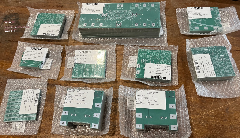 FYI Tracking - not updated since 5th not very impressive service, I don't like UPS ! Over a week to manufacture + 2 weekends, shipper notified on 25th for parcel pick up delivered 7th.... Edited 2024-11-07 16:49 by wiseguy If at first you dont succeed, I suggest you avoid sky diving.... Cheers Mike |
||||
| Cpoc Senior Member Joined: 28/05/2024 Location: PortugalPosts: 109 |
Ever since covid I find now shipping take twice as long to receive and now costs more than 2 X the price. This is everywhere in the world now. Transport costs is getting out of hand where sometimes it cost more to ship and item than the item itself. |
||||
| wiseguy Guru Joined: 21/06/2018 Location: AustraliaPosts: 1296 |
There has been a few questions about current Rev PCBs and other little issues so its time to update or and refresh some info for the latest WG (wiseguy) inverter PCB sets. Here is the BOM (bill of materials) for the WG39R7B nano controller, WG44R2 LCD & WG48R1 Front Panel. BOM WG39R7B WG44R2 WG48R1 120225.pdf And the BOM for the WG30R3 16 FET Power PCB & WG06R1 Capacitor PCBs 5KW WG30R3 & WG06R1 BOM.pdf I have also created a test procedure that brought my inverter to life and yes there were some silly issues, but nothing was damaged, the procedure tests all functionality and should not let out the smoke! For experienced builders it may probably be ignored - but I do recommend to use it, unsoldering from 2oz boards is not easy or fun. Inverter Test Procedure for initial tests of PCBs.pdf I would also like to revisit some advantages of the design/topology of the inverter that may not be obvious or has been long forgotten. With the ability to power the 16FET PCB from a variable power supply that is independent of the WG39 controller power supply and having the test link function it is possible to create opto drive signals for the FETs with the WG39 input voltage lower than the usual shutoff voltage and it ignores the difference between the Vin & Vcap voltages. What will happen with 0V applied to the FET power PCB, but the Nano controller (WG39) powered separately is the opto drive signals will achieve 99% modulation drive as the controller attempts to get enough feedback voltage from the mains for regulation. If powering for the first time or after a repair etc it is recommended to use the test WG06 capacitor PCBs loaded with a single 220u - 1000u capacitor each. The T4"A" & T3"B" terminals should be connected to a suitable choke and Toroid & with at least a 1uF capacitor across the mains output of the Toroid which is also wired back to J2 of the Nano controller. As the drive signal PWM is not clipping but is at maximum if we now apply 1VDC with a 100mA current limit into the FET power units T1+ & T2- terminals, we should see around 5VAC and the CRO should reveal a pretty good sinewave. The input current to the Power stage should be less than 100mA. Now increase the 1V slowly up to 50V (or 30 if that is your power supply limit). at 30V the mains should be typically ~ 150 - 160V - note at higher voltages the current limit might have to be increased to ~ 250mA. If you can increase the input voltage higher than 30V, then as you approach 40-45 volts (depends on actual turns ratio) the AC volts should become regulated and further increase of Vin, will not increase the ACV out any further. If all appears to be well then as a final test, wire up the WG39 controller J4 power input to the FET board power rails and now test again with a single power supply at 30/50 volts to T1 & T2 but with current at 250mA - 300mA and check for 150VAC or 230/240VAC depending on your 30/50 V power supply. If all is still testing fine it should be safe to put the normal WG06 capacitor boards back on the Power PCB and connect the inverter to a high current supply for further testing. At this point your warranty is void.....  For simplicity I have left out the second stage power and controller PCBs and also ignored the ACout OK relay drive connections to simplify the initial testing. Edited 2025-02-13 09:30 by wiseguy If at first you dont succeed, I suggest you avoid sky diving.... Cheers Mike |
||||
| wiseguy Guru Joined: 21/06/2018 Location: AustraliaPosts: 1296 |
Here is the BOM for the WG47Rev1 second stage controller. If faster turn on of the second stage is desired then R11 could be reduced to ie 1M or 470K for 1 second or 0.5 second delay before stage 2 starts. WG47R1 BOM 130225.pdf If anyone is also wanting updates for any boards modules etc not listed in this or the previous post please ask, also if there are any errors or omissions etc tell me as there are a few late nights in doing this half asleep, bound to be an error or two... If at first you dont succeed, I suggest you avoid sky diving.... Cheers Mike |
||||
| wiseguy Guru Joined: 21/06/2018 Location: AustraliaPosts: 1296 |
Time for a quick update. Latest project (pictured below) did not work first go!  I reversed one of the sides opto drives and it drove the transformer only in one direction for both halves of the 180 degrees, which after ~ 2 cycles the toroid was saturated and drawing bulk current, current limiting limit was set to a few amps so no damage. I reversed one of the sides opto drives and it drove the transformer only in one direction for both halves of the 180 degrees, which after ~ 2 cycles the toroid was saturated and drawing bulk current, current limiting limit was set to a few amps so no damage.Project is for a 12 - 230V inverter @ 2KW continuous for caravan use. PCB is 160mm x 100mm and made in 1oz. But the full length copper bus bars 3mm x 15mm should help a bit. I put the opto & buffer driver transistors on 2 small vertical PCBs which saved a lot of space. It has 12 Mosfets, (3 each leg of the bridge) I used the HY5608s as they are still excellent for this application. Idling at ~ 14.2W with 11V in and 230.5AC out unloaded. It looks like I may need to put another 10 to 15 turns on the output winding as it will droop a bit under load. The 2 cap boards can house up to 20 x 16mm dia caps on a 7.5mm pitch. Not sure what final value and quantity of caps I will use, still to be determined with more testing. Leaning towards a quantity of 8,200u @ 16V from digikey, with all 20 loaded ~ 700uOhms impedance. 2 different Cap PCBs and this power stage could also run off 48V, the 8 way opto/12V cable is still plug and play from the controller but as 2 x 4 pin cables. Ready for some serious testing soon. 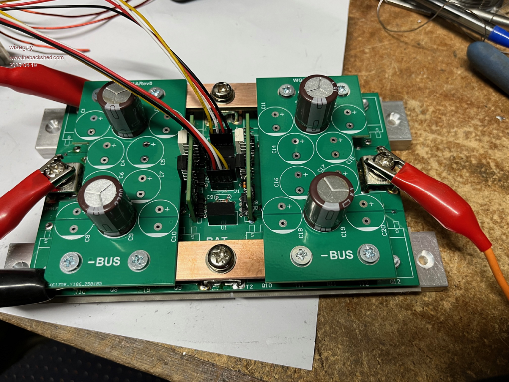 Now I can finally get back to the idling query of Oreos, but I had to clear the decks first. I note a few comments and replies about this subject from Nicks etc and I expect to confirm their comments that it is probably running fine. Edited 2025-04-19 19:19 by wiseguy If at first you dont succeed, I suggest you avoid sky diving.... Cheers Mike |
||||
| KeepIS Guru Joined: 13/10/2014 Location: AustraliaPosts: 2177 |
I just have to say it, that is one very sweet little Inverter board  NANO:Inverter V 8.2ks - Linux AvrDude GUI script V4.1 |
||||
| wiseguy Guru Joined: 21/06/2018 Location: AustraliaPosts: 1296 |
This was originally posted under MAB1's wiseguy inverter build here but it probably belongs here It may be helpful for some to discuss the startup circuit evolvement & issues. After re-reading Mabs comments I decided to take a trip back to earlier versions of startup to see what changed. When the controller was first designed all the voltage levels for the bulk capacitor voltage and Battery/Inverter main supply voltage were done via analog comparators. Thresholds were set by resistors and were a bit arbitrary. From memory if the bulk capacitors were within ~ 1 volt of the supply voltage the contactor was ok to close. Once Peter obliged me by modifying the inverter Nano code to include startup checks and validation checks, that could be user modified by a register value, such as voltage drop over the contactor contacts etc, the startup circuit - particularly the V+ (48V typically) became more critical as any voltage drop between the Vbat and controller 48V input could intefere with contact closure at startup and monitoring the Vdrop over the contactor contacts when closed. In trying to keep the startup circuit "simple" various insertions of diode and startup resistor combinations were tried, but the real problems was that in trying to simplify parts count it was a bit like putting lipstick on a pig. Somehow with a brain fart my schematic shown a few posts back from Mab 1 disobeys step 6 so the Nano will not ramp PWM down to zero due to a whoa camel stop event. (whoa camel was first mentioned a long time ago see here). The 48V is removed from the controller when "stop(off)" is selected due to the series diode - not good! (maybe also explains Mab's noisy contactor), the KeepIS configuration still feeds Vbat via the precharge resistor so the controller can reduce spwm to zero and shut down properly. Switching the run switch to stop causes the Nano's Vbat sense input to go low which reduces spwm to zero the same as the Vbat becoming too low. Fundamentally the main requirements are. Inverter is galvanically isolated from Vbat, now set the on off switch to "on" 1) Supply VBat (48V) directly to the controller so the nano sees Vbat exactly. 2) Simultaneously apply precharge to the bulk capacitors 3) When Vcap is high enough ~ close main contactor and run the inverter. 4) While inverter runs, monitor Vdrop across contactor (Vbat to Vbulk capacitor) 5) Now we want to stop the inverter, so set the on off switch to "off" 6) We need to maintain contactor closure and 48V to the controller. 7) Whilst contactor closed and controller has 48V, the spwm ramps back to zero. 8) Now with spwm=0, open the contactor and 48V is removed from the inverter & controller & contactor. 9) Ideally, there should be no sneak path from the Bulk capacitors back to the controllers Vbat input. With the KeepIS modification the controller is still connected/powered from the bulk capacitors after the main contactor opens, until their voltage has drooped enough to not support controller/display operation. The main benefit here is that the bulk capacitors are slowly bled away, however it may be possible for a few "flickers" as capacitors fluctuate towards zero. The first circuit shows a working configuration that I previously used, very similar to KeepIS. I am not advocating to use the second circuit it just shows an ideal solution. The second circuit could use either a spare contact set that some of the contactors use or alternatively a second small 48V relay driven in parallel with the contactor, untested but I believe it provides the required isolation from the bulk capacitors and the Nano controller. Note: the second circuit's bulk capacitors would stay charged for a very long time. Also note the prudent inclusion of the slow blow 1A fuse to the small toggle run/stop switch battery input (no doubt many have already done this). Apologies for the stuff up of what looked like a simple problem which got progressively worse. In summary unless you are having display flicker type problems IF using the KeepIS configuration dont bother with schematic 2. Anyone who has built their inverter with my schematic in Mabs post on the previous page should bridge/replace the diode with a short and supply the contactor direct from PWR48V (same as Vcap). 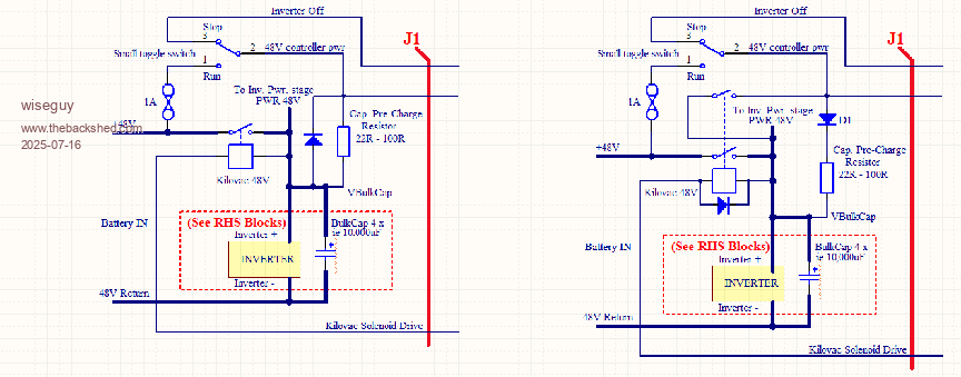 Edited 2025-07-18 10:54 by wiseguy If at first you dont succeed, I suggest you avoid sky diving.... Cheers Mike |
||||
| wiseguy Guru Joined: 21/06/2018 Location: AustraliaPosts: 1296 |
It has been an interesting journey on the back shed to develop this inverter. I have been pondering the inverter situation and where to go from here. In my personal life I fully retired in May last year, I have a lot on my bucket list and a lot of it requires travel. Now that there are a number of my PCBs in use in various locations around the planet, I feel a need to support constructors present and future in a way that does not have to involve me where my ability to help etc may be hamstrung if I am away or unavailable. Despite my reluctance to make publicly available the PCB manufacturing files there is now a conflicting requirement for them to be more accessible going forward. So I propose to figure out how to load them into JLCPCB's shared projects section so they can be ordered direct from JLCPCB. I don't propose to put the schematics & parts lists etc there, the forum members will know where to find any missing required information. I will probably list them as WG## numbers rather than 6KW home inverter. If I suddenly have a stroke or other mishap at least there will be support through future PCB availability. I discussed this in a recent email to another forum member, I will paste some of its contents here as it is topical. Paste: The Power boards really need to be manufactured in 2oz copper for the 5/6 KW rating, the capacitor PCBs I usually made in 2oz also. I think I should make all of the PCBs for the capacitor, display, Nano controller, second stage controller and maybe front panel available too. I don't intend to include schematics part lists etc the good guys on the forum that this is really for can already access these. FYI I got quotes for 5, 10, 15 & 20 off the Power PCBs including shipping the results are below WG30R2 PCB 5 = $100 total (inc ship $48) per ea $20.00 w/o shipping $10ea 10 = $121 total (inc ship $60) per ea $12.00 w/o shipping $6ea 15 = $132 total (inc ship $71) per ea $ 8.80 w/o shipping $4ea 20 = $198 total (inc ship $83) per ea $ 9.90 w/o shipping $5.75ea !! If the other various PCBs are purchased in prototype quantities (5) each type is under $7 (manufactured and delivered worldwide I believe), but if you were to add them to the Power PCBs order, freight can increase the overall freight cost rapidly. My advice, a few Aussies? get together and order the power PCBs to share the more expensive 2oz PCBs and the cost. Else if someone lives overseas just buy min. quantity of 5 & get over it, they now have 5 power PCBs for ~ $100! All the rest are best ordered by each person separately local or overseas, the cost of the remaining boards is then ~$35 total for the 5 types & 5 of each (a few spares). Lastly I have a confession, I am buying an inverter and batteries. 48KWH of batteries and a 25KW 3Phase inverter. The complexity of having a 3 phase house and wanting a fully automated set and forget system finally became more appealing to just order and write a cheque, the governments subsidy of batteries also helped with the decision. It will all be installed and commissioned probably in the one day before xmas. I am comfortable in my decision as I may well run out of time before I manage to spend all the kids inheritance. I intend to turn off the mains supply but still pay for the poles/wires for 12 months, If I have not had to switch back I will untether us from the grid after winter next year. Edited 2025-12-02 16:54 by wiseguy If at first you dont succeed, I suggest you avoid sky diving.... Cheers Mike |
||||
| Cpoc Senior Member Joined: 28/05/2024 Location: PortugalPosts: 109 |
Post some photos of the new inverter system when its up and running. |
||||
| rogerdw Guru Joined: 22/10/2019 Location: AustraliaPosts: 955 |
Hi Mike, glad to hear you've been enjoying your travels and planning more. I was a bit surprised to hear you've decided to buy a complete system, though can fully understand why. At times since I've had mine going I've thought it wouldn't be that hard to slot in some commercial equipment if I really had to ... especially when I've seen something cheap on marketplace or at an auction etc. Still kicking myself for not acting sooner when I saw a 48v 5kW Victron Multiplus and a couple of their charge controllers and more for $1,000. Would have been a very cheap backup system or start for someone else. Anyway, I like your idea of having your boards available directly from someone like JLCPCB. If anyone has ever considered building one, being able to quietly go off and purchase the necessary boards and go about collecting the parts ... and have a go at putting it all together may be very attractive. Then of course they could still ask questions here and get help if they needed it along the way. As you know, I'm in a facebook group of guys using forklift batteries ... and there is some interest there in building their own inverter as well. Many have bought the Ozinverter book from Leslie and are considering going down that track ... but I'd definitely be leaning them towards your new upgraded design ... especially now you can double up on the power board and aim for 12kW out. Anyway, let us know if you do put them up on JLCPCB and I'll let the group know ... and thank you for all your efforts and expertise in progressing the home made inverter scene. Cheers, Roger |
||||
| wiseguy Guru Joined: 21/06/2018 Location: AustraliaPosts: 1296 |
Hi Roger, unfortunately my memory seems to have let me down, I was sure it was JLCPCB that had the users projects section but it appears it was actually PCBWAY - at times I use either depending on price/time/capability/freight/etc, bat lately its like 80% to JLCPCB. So in light of this I have had a rethink and propose the following solution. I should just place access to the gerber files in my next post here on the forum. Then everyone/anyone will have access to the files necessary for manufacture and be able to choose their favourite/local PCB Maker to obtain their PCBs & perhaps save freight, duty, and similar issues as well. It would be good if we could have the ability for file links like this to designate them as public/private so joining the forum is required before making them available for viewing or downloading to random guests. Ultimately this might be good for the forum generally as well. If at first you dont succeed, I suggest you avoid sky diving.... Cheers Mike |
||||
| rogerdw Guru Joined: 22/10/2019 Location: AustraliaPosts: 955 |
Yes, it could be quite convenient if it was set up that way ... and would have to be good for the forum too. Or maybe you could add them to your signature like KeepIS has done. Not sure how but obviously it's possible. Cheers, Roger |
||||
| wiseguy Guru Joined: 21/06/2018 Location: AustraliaPosts: 1296 |
The Sigenergy system went in today and was finished ~ 5.00pm. The batteries were only 40% charged and currently we are running our house including ducted air on the sig system. Now the air conditioning has ramped down to maintain temperature Power reduced from just over 7kW down to 2kW. The system now has 12.9kW (26%) remaining so in theory if nothing changes, we have ~ 6 hours remaining. However, as the evening cools, the air cant ramp down much further so it starts to cycle off for longer periods so I expect it to not actually draw from the mains tonight - we will see. Batteries should reach 100% for the first time by about noon tomorrow. As far as pictures go there is very little to see. In the garage we have the Sig "gateway" which is a fancy name for wireless monitor of AC street info, AC from Sig and AC to the house. It provides islanding from the street power when there is no power but otherwise it is ready to use street power to supplement our inverter/batteries if the Solar/batteries cant keep up with the load (greater than 25kW). The rest is a stack of 6 x 8kWH modules topped off by the 25kW 3 phase inverter unit with 4 x MPPT's inbuilt. The final picture shows the eaves / top of sig stack, should I put an angled metal shield, bolted to the wall, between the sig stack and the eaves to deflect heat and flames outwards past the eaves just in case??  Gateway unit: 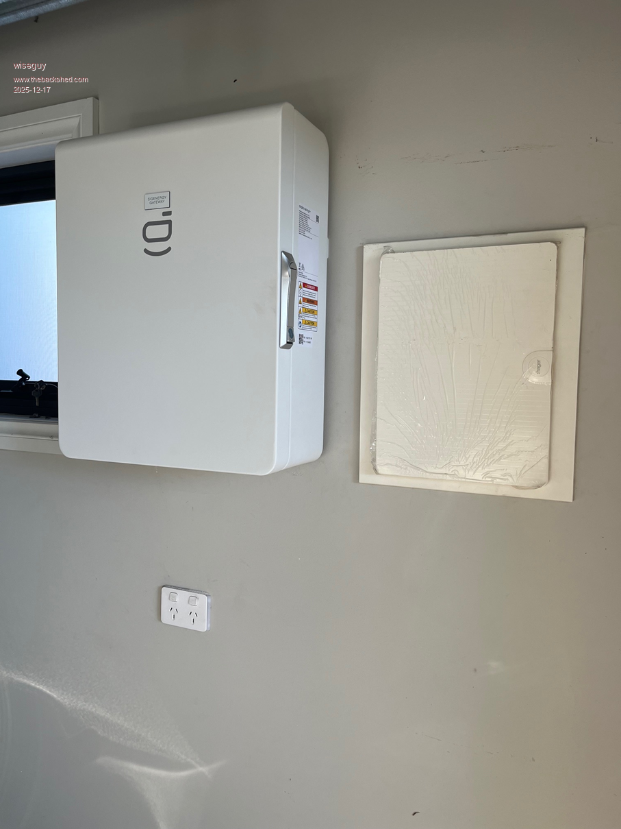 Outside stack: 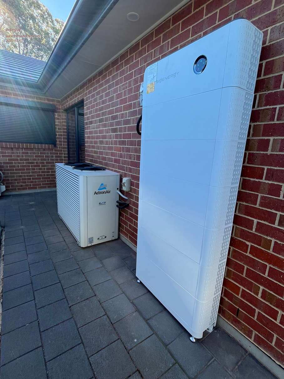 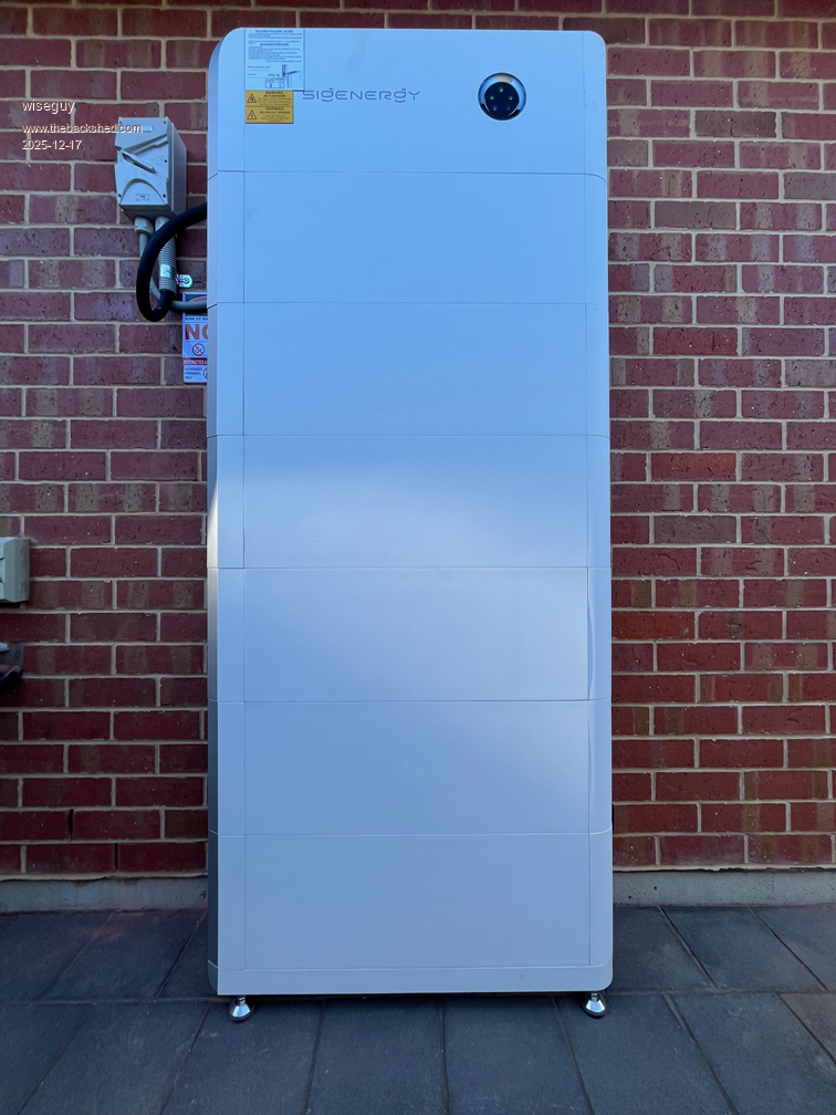 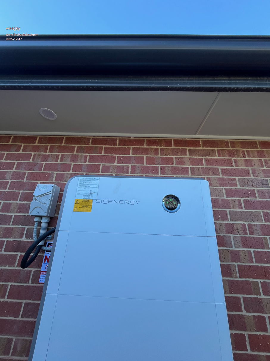 Edited 2025-12-17 20:27 by wiseguy If at first you dont succeed, I suggest you avoid sky diving.... Cheers Mike |
||||
| The Back Shed's forum code is written, and hosted, in Australia. | © JAQ Software 2026 |
