
|
|
Forum Index : Microcontroller and PC projects : My God, there are a lot of them....
| Author | Message | ||||
palcal Guru Joined: 12/10/2011 Location: AustraliaPosts: 2039 |
@redrok Have a look on geoffs website at the Micromite LCD Backpack. Those Mosfets would be no good but thought the circuit may help. Paul "It is better to be ignorant and ask a stupid question than to be plain Stupid and not ask at all" |
||||
| flip Senior Member Joined: 18/07/2016 Location: AustraliaPosts: 119 |
+1 Panky & Redrok's mod (Zener not needed but some people may feel safer with it there) & Panky's arrangement makes the design virtually independent of how high the upper voltage is (all the strain taken by the NPN)..(of course as long as supply not connected backwards) Very clever & simple, Phil |
||||
| robert.rozee Guru Joined: 31/12/2012 Location: New ZealandPosts: 2499 |
i'm pretty sure the zener needs to remain, it is the key component ensuring Vgs does not exceed 8 volts. without it the maximum Vgs applied is determined by the ratio of R1 to R2, which is a risky approach. as per my earlier suggestion, R1 can be increased to 3k3, this will give a maximum current sink of 800uA. this should be sufficient to keep the zener more-or-less happy (it will be operating a bit down the voltage curve, but that doesn't matter). at the same time i've decided i'd like to increase R2 to 100k - this will ensure that the majority of that 800uA flows through the zener. with the original R1 = 330 ohm, there is the potential for sucking 8mA out of the micromite's pin if the 12/24v supply is missing. while within the drive ability of the micromite, this is untidy. btw, note that no base resistor is needed for Q1, as the base current is limited by the value of R1. basically both collector and base currents flow through R1, being limited to Ie = (3.3-0.6)/R1. as long as the collector current can flow (the zener is conducting) the base current will be negligible. cheers, rob :-) |
||||
Grogster Admin Group Joined: 31/12/2012 Location: New ZealandPosts: 9932 |
I'm inclined to agree with Rob. The DMP2305 MOSFET has a MAXIMUM Vgs of 8v. I read that to mean that if you put a potential of greater then 8v across the gate, you will destroy the oxide layer, and kill the transistor. I am still a novice with MOSFET transistors, so I may have that wrong for some reason others would like to explain here.  Could you use a potential-divider on the gate, to set the gate voltage to whatever you needed it to be(no zener then), and then pull the gate low with the NPN? Like this: 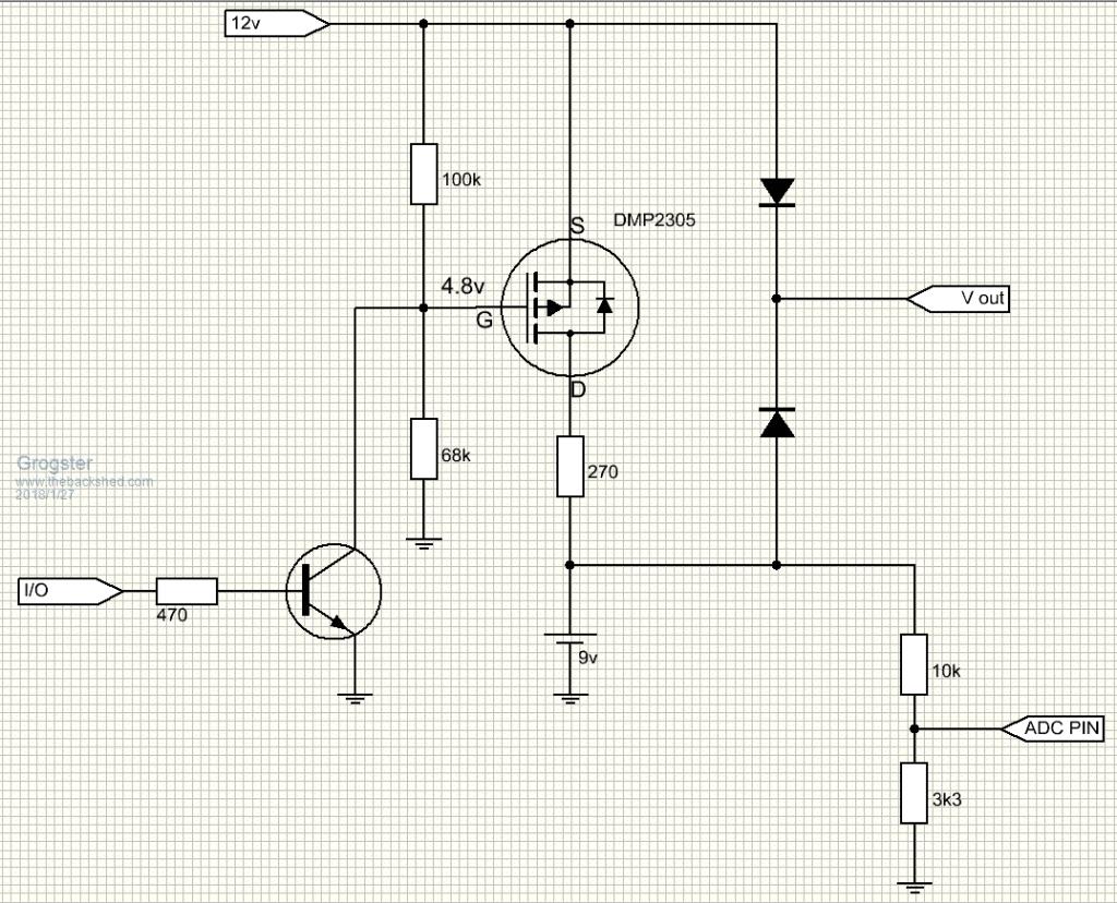 Smoke makes things work. When the smoke gets out, it stops! |
||||
| robert.rozee Guru Joined: 31/12/2012 Location: New ZealandPosts: 2499 |
no, that will leave the mosfet permanently turned on. i see redrok's reasoning for leaving out the zener now (4mA * 1K = about 4V Vgs) but think i'd still leave it in there myself (with R2 = 100k) instead of saving a few cents. cheers, rob :-) |
||||
| Grogster Admin Group Joined: 31/12/2012 Location: New ZealandPosts: 9932 |
Acknowledged. Smoke makes things work. When the smoke gets out, it stops! |
||||
redrok Senior Member Joined: 15/09/2014 Location: United StatesPosts: 209 |
I for the life of me can't see a reason for the zener in this circuit. 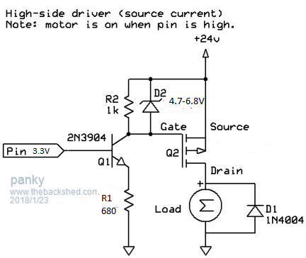 I will explain why: 1. First the use of 680R driven from a 3.3V pin would normally cause about 4mA to flow through it. (3.3V - 0.6V) / 680R = 3.97mA With a transistor gain of 100 the base current would be about 40uA when sourced from the 3.3V pin. At worst case, when the relay supply is turned off. (3.3V - 0.7)/680 = 3.8mA base current sourced from the 3.3V pin. Now if the relay supply is turned on instantly the 2N3904 with a 4mA base current could attempt to sink about 120mA for a few nS. However, the 2N3904 has a 300mHz gain bandwidth product, and a high current gain of 30, so at best it could do this for only about 30 * 4mA = 120mA with an instantaneous base current of 4mA 3nS * 120mA/8mA = 45nS to get past 8V. If the relay supply ramps up faster than 45nS there could be a problem. 2. But the DMP2305 MOSFET has quite a large gate capacitance of about 730pF. 730pF * 8V / 120mA = 49nS Total = 94nS 3. But wait, there is capacitance between the drain and gate of 64pF, the Miller Capacitance. As the DMP2305 is turning on it injects current back into the gate effectively increasing the gate capacitance by 730pF * (1 + 64pF/730pf) = 794pF effective gate capacitance. 794pF * 8V / 120mA = 53nS Total = 98nS any supply ramping up faster than this could cause a problem. Remember, this is for a Relay Supply turning on instantly(< 1ns) and with the instantaneous base current of 4mA (Which it will not, and rapidly decrease to 40uA). It's hard to believe the 2N3904 wouldn't have time to stabilize the current sink current to 4mA in 100nS. Probably much faster making things safe even quicker. Of course, the relay supply will take even longer to come up to voltage than 100ns, probably several uS to mS. So there is no way the gate can see more than 8V and fail. 4. This calculation was based on the transistor "Remembering" it had a 4mA base current. Of course 120mA could not possibly flow through it. The absolute maximum would be limited to what the resistors would allow: 12V / 680R = 17.6mA worst case current. and dribble down to 12V / (1000R + 680R) = 7.1mA until the transistor is stabilized. Averaging about 12mA The time to charge the gate capacitance to 8V would be about 10 times longer than the 100nS, above, or about 1uS or so. Actually it will take longer to charge the gate capacitance because the base is "forgetting" the 4mA base current and reverting back to 40uA base current. At 4mA sink current I suspect it would take more like 2uS to get the gate to 4V. This high gate capacitance is why MOSFET drivers often need to drive several Amps to switch them fast. The stabilization time to 4mA sink current would be much faster than 1uS, probably 10ns to 40nS or so. Can you turn on the relay supply that fast, I don't think so, especially if there is a reasonable filter cap on the buss. If you feel safer with the zener, by all means use it. The value should be between 4.7V and 6.8V, I would think. I would use the 1N57xx series of low power zeners as they turn on faster than the 1N46xx 1W zeners. But I don't think you need it. BTW, this is the worst possible scenario, micro on before relay power is applied, as all others start out with no current flowing. redrok |
||||
| Zonker Guru Joined: 18/08/2012 Location: United StatesPosts: 772 |
Evening Gent's.. I was just wondering if anyone has tried using this part... I have, and it works quite well for all kinds of things... The VN7003ALH high side driver IC may cost a bit more BUT... I solves many of the problems that I was having and the pins just connect up to the MM and you got it... This thing IS bullet proof... NO Really..!! It is... It has many advantages already built in. 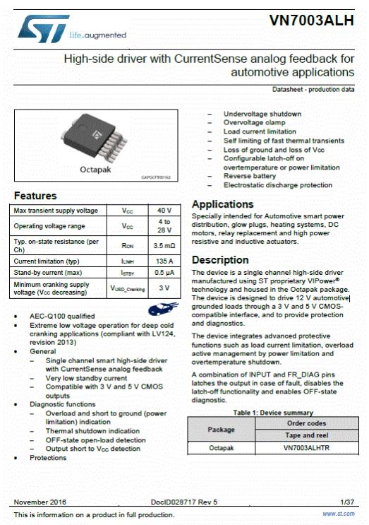 Just drop in a resistor to set the scale, and you can measure the current.. Works great with PWM and is made to drive big inductive loads with ease... The MM interface is totally protected from the HV driver side... |
||||
| Grogster Admin Group Joined: 31/12/2012 Location: New ZealandPosts: 9932 |
Very interesting device!  Link to PDF. Smoke makes things work. When the smoke gets out, it stops! |
||||
| Boppa Guru Joined: 08/11/2016 Location: AustraliaPosts: 816 |
Mouser(.au) have them on a pcb for $5.76, but I havent found them anywhere else yet Looks like a brilliant little chip indeed I like the feedback system, I'm making a combination gate/garage door opener system, and if it works as I think it does, it even will give blocked closing monitoring- sweet.... |
||||
| redrok Senior Member Joined: 15/09/2014 Location: United StatesPosts: 209 |
Hi Zonker;I haven't myself. But have used a few P-Chanel versions in the past. BTW, these are called "High Side Switches", not "High Side Drivers" which use external MOSFETs. There are quite a few "High Side Switches" out there. STMicroelectronics has many in their line. Single, Dual, and Quads. These are "AEC-Q100 qualified", basically designed to be used in the horrendous automotive environment where the voltages can go sky high and even go reversed during "Jump Starting". For our more "Normal" usage we may not need some of the external zeners and other protections. I suspect no external components, except for the current programming resister, are needed. I can't see, from the specs, how they generate the high side voltages for the N-Chanel gate? I suspect their using a capacitive voltage boost circuit on the chip. I don't think this device requires the load be periodically switch to maintain the high side voltage. It seems the MOSFET could be switch on continuously. Almost as if it were DC coupled. Is this true? redrok |
||||
| LouisG Senior Member Joined: 19/03/2016 Location: AustraliaPosts: 130 |
Have you considered using solid state DC-DC relays? They can easily be arranged for high side driving. I think they use photo-voltaic couplers to provide isolation and generate the MOSFET gate drive voltage. I suggest to stick to your quest for high side switching. High side is good for everything. Low side is good just for isolated, non-polarised two-wire devices. Wait till you get a mix of conventional solenoids, polarised solenoids (e.g in contactors) and 3-wire devices such as small motorised ball valves, which can only accept a ground referenced positive signal. |
||||
| The Back Shed's forum code is written, and hosted, in Australia. | © JAQ Software 2026 |
