
|
|
Forum Index : Microcontroller and PC projects : Well, apparently I have killed my unit.
| Author | Message | ||||
| yock1960 Senior Member Joined: 18/08/2020 Location: United StatesPosts: 167 |
Well, C5 was easy to get off....the regulator...not quite as easy. One of the traces tore loose a bit...is that fatal? Steve 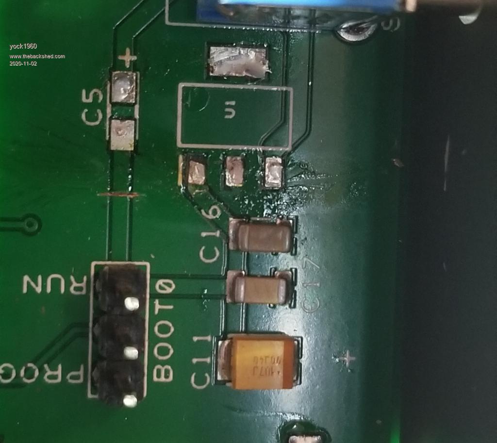 |
||||
| yock1960 Senior Member Joined: 18/08/2020 Location: United StatesPosts: 167 |
I just checked and I have continuity between the damaged trace/pad and C16, with the other end trace and the + side of C5...I guess I'll look at the schematic to see if I can figure out where the other two pads go to and check those....and order a couple of regulators. Steve |
||||
| yock1960 Senior Member Joined: 18/08/2020 Location: United StatesPosts: 167 |
https://www.mouser.com/ProductDetail/ON-Semiconductor/NCP1117ST33T3G?qs=Gev%252BmEvV0iZb%2FE8ahUDx3w%3D%3D&gclid=Cj0KCQjwufn8BRCwARIsAKzP695AA5cIpGLsd6kGw5OeeOEw8ujj_cSA0880gLWBDlFzfWAEqa7BrwgaAhafEALw_wcB Is this an appropriate replacement? It cam up when I Googled AMS 1117, which is what's printed on the chip. Steve |
||||
TassyJim Guru Joined: 07/08/2011 Location: AustraliaPosts: 6538 |
The damaged pad doesn't look too bad. I have seen a lot worse on some I have done. The AMS1117 is the same as the LM1117. Either will do but make sure it's the 3.3V version. They both come in a number of different output voltages. The one you linked to is correct. The two pads you haven't traced/checked yet are both the 3.3V output and are connected to the top side fill area. You should be able to see the small links from the pad to the fill. The small links are used to give thermal separation from the big copper ares. If the connection is too big, it makes them hard to solder. Jim VK7JH MMedit |
||||
bigmik Guru Joined: 20/06/2011 Location: AustraliaPosts: 2981 |
Hi Yock, All, I would be extremely careful with the damaged pad as it is the GND pin and the top layer cooper pour is actually on Vcc. If it was me I would cut the pad away so there is no loose track or pad even left. Then solder an LED wire or stiff single core wire from the leg of the replacement Vreg to the side of C16 that the trace would have gone to. Making sure there is no possibility of shorting to the copper pour area..USE A METER to test that the fix is clear of the vcc pour. I would offer to repair it for you but it would be expensive to ship 2 ways and probably a good month turn around.. But I will do it for you if you wish. Regards, Mik Mick's uMite Stuff can be found >>> HERE (Kindly hosted by Dontronics) <<< |
||||
| yock1960 Senior Member Joined: 18/08/2020 Location: United StatesPosts: 167 |
So if I understand you, your concern is shorting the new solder/leg on the layer under the torn area? Could I not place some insulating material under that torn spot? To prevent this shorting. LED wire? I don't see any single core wire in my parts bin...I do have some fairly stiff 7 strand copper twist, it's not labeled, but looks like it would be 16 or 18 gauge on the wire stripper. Steve |
||||
| Mixtel90 Guru Joined: 05/10/2019 Location: United KingdomPosts: 8911 |
How about just stabilising the loose track with a spot of superglue from a toothpick, making sure it's in the right position. Solder the new reg in afterwards once it's stuck down. IMHO putting a wire link in might be more difficult. Dabbing a wire on anywhere along that ground line would run the risk of shorting it to + anyway. The solder mask will help, of course, just as it will in the reg position. Plenty of flux and some quick soldering. Mick Zilog Inside! nascom.info for Nascom & Gemini Preliminary MMBasic docs & my PCB designs |
||||
| bigmik Guru Joined: 20/06/2011 Location: AustraliaPosts: 2981 |
Hi Yock, All, My concern is the large area of copper that flows around all of the pads on the TOP layer is connected to VCC IF the loose trace moves and touches this copper area (called copper pour) then you will short Vcc to GND. You 'could' possibly glue the pad back but the trace has been compromised and really should not be relied on especially as this VReg supplies all of the 3v3 power to the CMM2. I said LED leg as it is generally a bit thicker than a Resistor or capacitor leg, I would avoid braided wire as a stray strand could find its way through to the copper pour.. Solid strand is easier to solder anyway. I dont know what your skills at soldering are like and your confidence level.. You will have to make the assessment of the best procedure for yourself. I mentioned adding the wire as WHAT I WOULD DO to fix the problem. If you dont feel confident surely you have a friend who might be able to assist with the repair or at worst case ship the bare PCB to someone who volunteers to look at it for you (presumably locally). I am happy to have a look at the job for you but shipping a board from AUS to USA would cost probably $12 (no tracking no insurance and would take 2 -3 weeks) and I dont know about cost or delays from USA to AUS. Kind Regards Mick Mick's uMite Stuff can be found >>> HERE (Kindly hosted by Dontronics) <<< |
||||
| yock1960 Senior Member Joined: 18/08/2020 Location: United StatesPosts: 167 |
Thanks for the input Bigmik & Mixtel90! After watching some videos, I'm reasonably confident that I can do this....and if not...my insurance policy...Retromax shipped today. Steve |
||||
| TassyJim Guru Joined: 07/08/2011 Location: AustraliaPosts: 6538 |
Not going to the races today Mick? It's bloody hard fixing by remote control. Teamviewer hasn't got that good yet. I would also do some measurements on the 3.3V side before replacing the regulator and probably feed it with an external 3.3V supply, suitable overload protected. Resistance between 3.3V and ground should start at a low value then increase as the capacitors charge up. Put the positive multimeter lead to 3.3V. It is something that the good old analog meters do better than the digital ones. Once the regulator has been replaced, I wouldn't like to try it a second time. Jim VK7JH MMedit |
||||
| TassyJim Guru Joined: 07/08/2011 Location: AustraliaPosts: 6538 |
I would run a scraper down the edges of the track you cut earlier. What Mick is correctly worried about is shorting the trace which is ground to the copper fill area which is 3.3V  The area circled looks a bit suspicious. Jim VK7JH MMedit |
||||
| bigmik Guru Joined: 20/06/2011 Location: AustraliaPosts: 2981 |
Hi Jim, All, Nope! Firstly I retired just over 2 years ago, Secondly due to Covid19 there are no punters at the races, hence no on course betting so I wouldn't have been there anyway.. I went to 32 Melbourne Cups (Most famous Horse race in Australia) in my 33 years on `totes' I missed one due to my health and one due to my wife's health but I feel 32 was a decent innings in my 33 years on the job. @YOCK I have been considering what might be wrong with your CMM2 by reading and re-reading your posts.. I suspect it is the VReg as the voltage values were way wrong. Another thought (unlikely due to voltage readings) I wonder if after you flashed the newer firmware with the A-A cable (not sure how that worked with a crook 3v3 supply) did you put the link back into the RUN position? The response you would get if you didn't is more or less the response you reported after doing the flash of firmware if the link was still in the PROGRAM position. When you get your Retro-Max, if you cant find someone locally, I am happy to look at your board for you.. Just ship the PCB (no case) and at cheapest post and I will ship it back the same way, after all the pressure of time is not there with your New MAX. Kind Regards Mick Edited 2020-11-03 11:23 by bigmik Mick's uMite Stuff can be found >>> HERE (Kindly hosted by Dontronics) <<< |
||||
| yock1960 Senior Member Joined: 18/08/2020 Location: United StatesPosts: 167 |
In light of TassyJim's concerns above, can I do something like this? Scraping a small section of the trace, soldering there and being very careful not to get solder in the cut. Steve 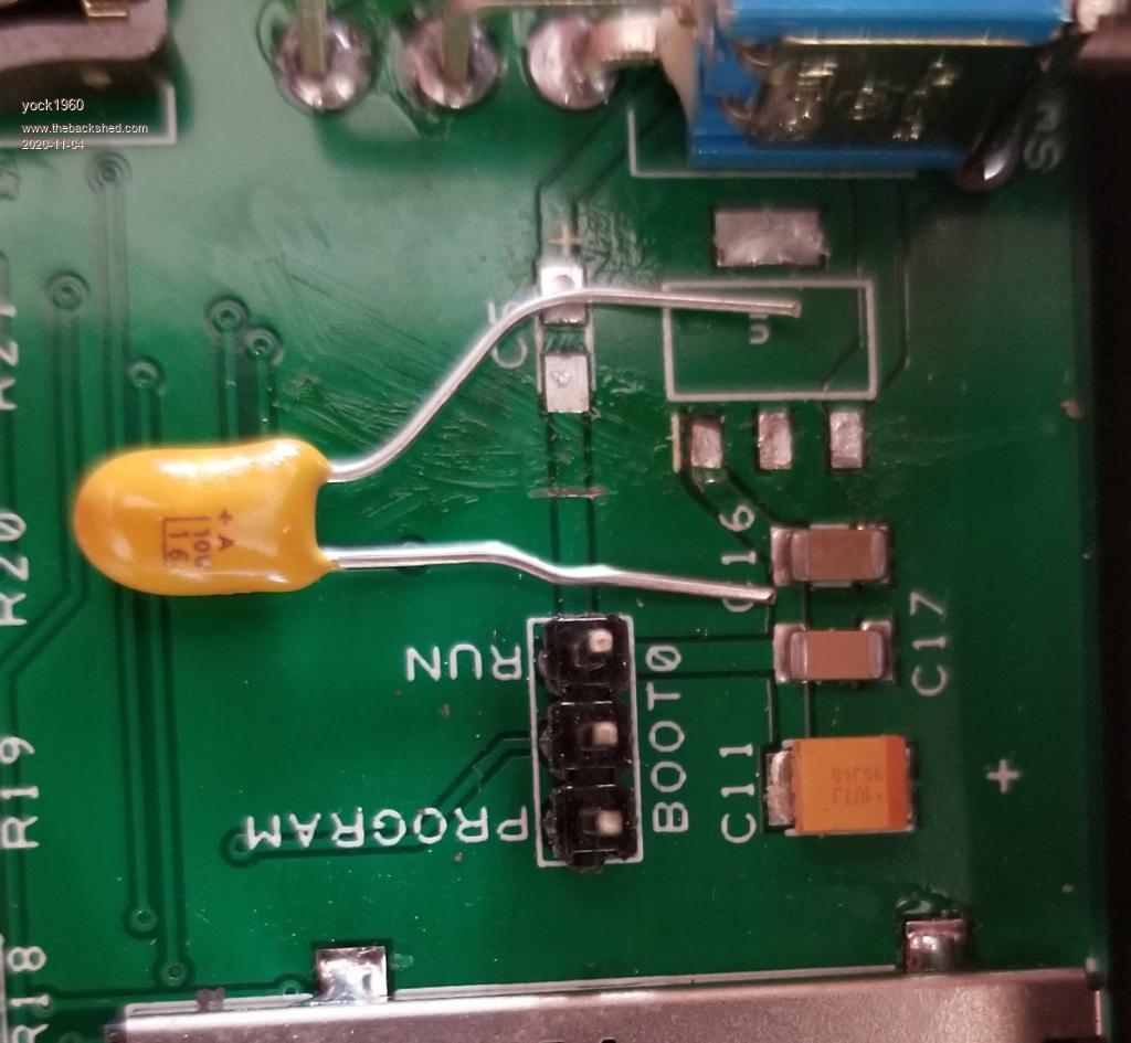 |
||||
| matherp Guru Joined: 11/12/2012 Location: United KingdomPosts: 11512 |
Solder a new regulator on and if you have a clean supply you can probably ignore C5 completely. Certainly no issue testing without it |
||||
| yock1960 Senior Member Joined: 18/08/2020 Location: United StatesPosts: 167 |
A dirty supply would result in...instabilities? As it was, I would see random failures to open modfiles and with the mouse adapter I was getting what THWill calls this system's blue screen of death errors, so...well I guess I try it and see...if it's no worse, then it's still a win and if it's worse, I add C5. Steve |
||||
| matherp Guru Joined: 11/12/2012 Location: United KingdomPosts: 11512 |
A dirty supply would result in...instabilities? The regulator going into oscillation. The LT1117 specifies a capacitance of 10uF on the input. But if you have a smoothed supply with some output capacitance then it should be happy as long as the leads aren't too long |
||||
| TassyJim Guru Joined: 07/08/2011 Location: AustraliaPosts: 6538 |
It is the vertical gaps either side of the original trace that worries me. When you did your horizontal cut, it looks like there are some copper dags that were left at the ends of the cut. A quick scrape down the vertical gaps will ensure that they don't bridge to the copper fill area. Your capacitor lead would be a good candidate for using as a solder aid if required but your cut is nice and narrow so it shouldn't be needed. At Peter suggests, try without the capacitor first. If it doe work than consider the capacitor as a second step. Jim VK7JH MMedit |
||||
| yock1960 Senior Member Joined: 18/08/2020 Location: United StatesPosts: 167 |
Jim, Could you make a sketch on one of the photos to illustrate what you mean? My original understanding, before I knew about 'copper pour', was that I would be scraping off some solder mask on either side of the cut, then bridging the gap with solder. Now, my...less than complete understanding, needless to say, is that perhaps I cut too deep, getting into the copper pour and my bridging solder would potentially short this trace to that. Maybe this was inevitable, maybe not...but given this, I'm not getting your 'scrapes on vertical gaps' and what this would accomplish. Sorry to be so dense...but this kind of stuff is a bit beyond my experience! Thanks! Steve |
||||
| TassyJim Guru Joined: 07/08/2011 Location: AustraliaPosts: 6538 |
My description is not the best. In this photo, 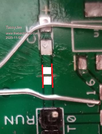 Run a scraper over the gap marked in red to make sure that there is no stray bits of copper that always appear when you do a cut. I can usually feel the scraper catching on the copper bits as I drag across the area. Do this before starting to solder and there will be much less chance of solder running where you don't want it. Then, scrape off the solder mask from the area in white ready for soldering. The bare copper exposed should be easy to solder to and provided you don't use too much solder, it will not spill over onto the unwanted areas. If it does, a clean iron without any solder will usually take back any surplus solder. Jim VK7JH MMedit |
||||
| yock1960 Senior Member Joined: 18/08/2020 Location: United StatesPosts: 167 |
Capeesh! Thanks! Steve |
||||
| The Back Shed's forum code is written, and hosted, in Australia. | © JAQ Software 2026 |
