
|
|
Forum Index : Microcontroller and PC projects : MicroMite+ Explore64 PCB 1C...
| Author | Message | ||||
Grogster Admin Group Joined: 31/12/2012 Location: New ZealandPosts: 9975 |
@ Chris - Yeah, see what you mean. I normally just let the weight of the PK3 hang at the right angle, and it stays there long enough to program the firmware in. I don't mount any pin-strip on the ICSP holes. Anyone else like Chris's idea? Smoke makes things work. When the smoke gets out, it stops! |
||||
| Grogster Admin Group Joined: 31/12/2012 Location: New ZealandPosts: 9975 |
UPDATE @ Rob - Like this? 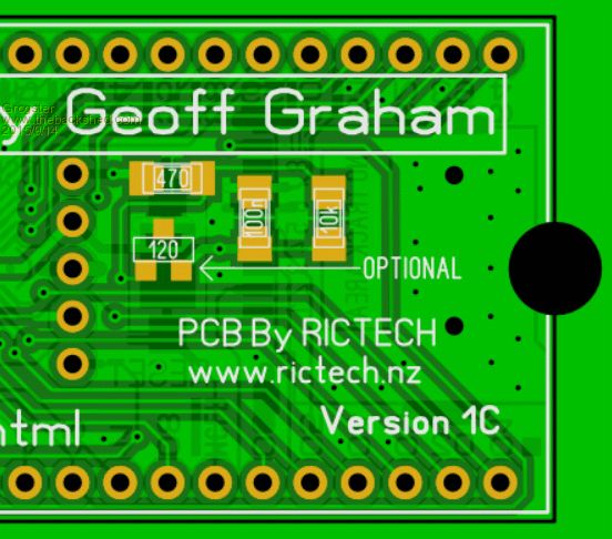
EDIT: Oh, you also asked about the 120 vs 130. The 120 needs the 10k pull-up, but the 130 has a pull-up built in, so by using the 120, you can either just have the 10k pull up, or both for full supervisory control. You can also use the 130, just don't install the 10k. ...and the extra GND around the USB socket... 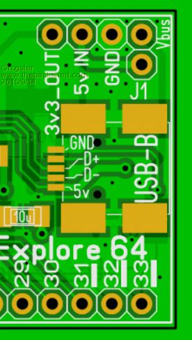
Smoke makes things work. When the smoke gets out, it stops! |
||||
| WhiteWizzard Guru Joined: 05/04/2013 Location: United KingdomPosts: 2991 |
To be clear, the staggered pins allow you to not have to solder anything in the PCB. Then with a PicKit3 (or other programmer), you simply put a temporary 5-way (or 6-way) male header into the PicKit female socket, then push-fit this into the PCB's staggered pins. There is enough 'friction' to hold it firmly in place while updating firmware. Then simply remove all. Another benefit is that it can keep reduce module height . . . I am a big fan of these staggered ICSPs 
WW EDIT: I know you can do the same without staggering the pins BUT there is a chance of a failed 'update' due to things moving. For no extra board space, these pins are worth staggering. NOTE: You can still solder in a row of pins into staggered holes if you wish  |
||||
| Grogster Admin Group Joined: 31/12/2012 Location: New ZealandPosts: 9975 |
Hokey pokey. I will make that change. Smoke makes things work. When the smoke gets out, it stops! |
||||
| robert.rozee Guru Joined: 31/12/2012 Location: New ZealandPosts: 2527 |
yep, what you've done in the area of the supervisory chip is what i had in mind. i would still leave a little thermal relief around the GND pin on the USB socket, solid copper on three sides may suck away the heat just a little too effectively when trying to hand solder. you could also add an extra via to the end of the track that connects the 5v pin to the underside of the board, so there are two vias carrying the load, but that is fairly minor. cheers, rob :-) |
||||
| Grogster Admin Group Joined: 31/12/2012 Location: New ZealandPosts: 9975 |
Is this staggered enough? 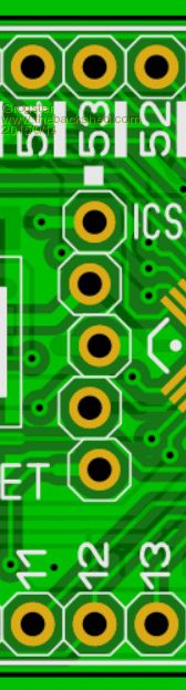
Smoke makes things work. When the smoke gets out, it stops! |
||||
| MicroBlocks Guru Joined: 12/05/2012 Location: ThailandPosts: 2209 |
The holes for the plastic 'feet' of the USB connector are those standard pads? If so, you could add them to the GND net so that they not break the ground lines. I mean the two pads that are next to the silkscreen text where it says 5v and GND And if i look good i think with the wavy pattern of the icsp only the top pad is not lining up with the rest. @Chris, how much distance are the pads to the left and right from the center line? Is this the same pattern as Sparkfun used? Also what hole sizes are used. Another advantage, the reason it was 'invented', is that when you need to solder a lot of pinheaders, they just stay in place. I am interested in using this for my blocks too, a simple but very effective way of mounting the headers, i simply forgot about it and used the provided patterns with my pcb design program. .....i am of to go change all those patterns right away.' 
Thanks for bringing this up Chris. Really just on time!  Microblocks. Build with logic. |
||||
| robert.rozee Guru Joined: 31/12/2012 Location: New ZealandPosts: 2527 |
i would be a little bit cautions about the zig-zag pins, just a fraction too much zig, and the connector may not fit in. an option that i've seen used before is to use a machine-pin header/socket where a low profile is desired. a matching adapter can be made with a pin header soldered to the top of a second set of machine-pins. cheers, rob :-) |
||||
| Chris Roper Senior Member Joined: 19/05/2015 Location: South AfricaPosts: 280 |
To be honest I don't know the actual offset or diameter, I have only ever used them, not manufactured them. The boards I have that use this are all from Digilent but I am sure the Sparkfun version is probably the same. I may have, or be able to get, the Digilent artwork files if that will help. It is only slightly offset, just enough to create friction but not prevent easy insertion. Cheers, Chris http://caroper.blogspot.com/ |
||||
CircuitGizmos Guru Joined: 08/09/2011 Location: United StatesPosts: 1427 |
Here: https://www.sparkfun.com/tutorials/114 Micromites and Maximites! - Beginning Maximite |
||||
bigmik Guru Joined: 20/06/2011 Location: AustraliaPosts: 2981 |
Lads, This is an interesting Proposal, one I have never heard of before, My first thoughts are Fantastic, Great idea but on reflection I feel it could be dangerous if there are manufacturing errors or inaccuracies in hole sizing etc. You may get a situation where the pins dont fit in the holes at all or still are too loose to touch all pads without applying - Angular - pressure, as is the case without the offset. I think that Robert's idea is a safer option, you can also use low profile FEMALE headers (these come in certainly 5mm size which is basically the height of the USB connector and Crystal) then all height problems are basically non-existant. Regards, Mick Mick's uMite Stuff can be found >>> HERE (Kindly hosted by Dontronics) <<< |
||||
| Grogster Admin Group Joined: 31/12/2012 Location: New ZealandPosts: 9975 |
PERSONALLY, I prefer the holes all in-line, and not staggered, but I am open to the suggestion. I think the risks of the pins not fitting in the staggered arrangement if only out by a tiny amount, are a really relevant point, so at this stage, I am going to put the pins back in-line as normal. As mentioned, I have not had any issues programming by just making sure there is some sideways tension on the PK3 programmer cable. Not bumping the unit while programming is not a problem in 99% of the cases I would think, as it only takes moments to program. Perhaps it would be a better idea, to put the pins back in-line, but make the holes just a tad smaller - they are 1mm at the moment, so if we went down to 0.8mm and in-line, the pins should be a better "Fit". Smoke makes things work. When the smoke gets out, it stops! |
||||
BobD Guru Joined: 07/12/2011 Location: AustraliaPosts: 935 |
Grogs I won't work. I just measured some pins and they are all about 24 to 24.5 thousandths of an inch square. Calculate that out and it comes to 33.94 thous. across the diagonal. I measured across the diagonals (the limiting factor here) and got a measurement of about 33 thous. 0.8 millimetres is 31.49 thous. You would have what could be called an interference fit. 0.9 mm is 35.49 thous. You could get away with that. So why work in inches. The measurement precision in millimetres is 0.1 which is approx. 4 thousandths. we get 4 times better precision in inches. It's a limitation of the measuring gadget. Bob |
||||
| WhiteWizzard Guru Joined: 05/04/2013 Location: United KingdomPosts: 2991 |
Just woke to this debate about staggered pins! The offset you have between pins 1 & 2 are fine (the other pins may be too much). Just take a look at the spark fun library in Eagle. Under connector section look for 1X05_LOCK_LONGPADS Used many times and works really well . . . . WW |
||||
| bigmik Guru Joined: 20/06/2011 Location: AustraliaPosts: 2981 |
Grogs, I always use .038" as my hole size, The square pins are a loose fit so you prob could drop to .036" dia. Mick Mick's uMite Stuff can be found >>> HERE (Kindly hosted by Dontronics) <<< |
||||
| paceman Guru Joined: 07/10/2011 Location: AustraliaPosts: 1329 |
Grogs, Here's just a quick comment because it won't changed any functionality but it might facilitate discussion or trouble-shooting anyone's possible problem with the board. How about silk-screening an ID (are they called Reference Designators?) to the resistors and capacitors. Just R1, C1 etc. so that the circuit and any changes can be easily described. Once a user has installed the components they can't see their values and if the component's not marked it's long-winded to describe - e.g. "the resistor just left of the USB connector" - instead of just "R3". I had a non-expert look at the layout and it doesn't seem that would be difficult to do anywhere. Greg |
||||
| Grogster Admin Group Joined: 31/12/2012 Location: New ZealandPosts: 9975 |
Good idea, Greg. I will add that to all components. Smoke makes things work. When the smoke gets out, it stops! |
||||
| Grogster Admin Group Joined: 31/12/2012 Location: New ZealandPosts: 9975 |
Nice spotting. I have made the change. I have put the ICSP back to being in-line, but have made the holes 0.9mm instead of 1.0mm.
TOP: 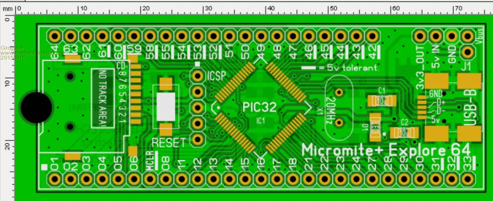
BOTTOM: 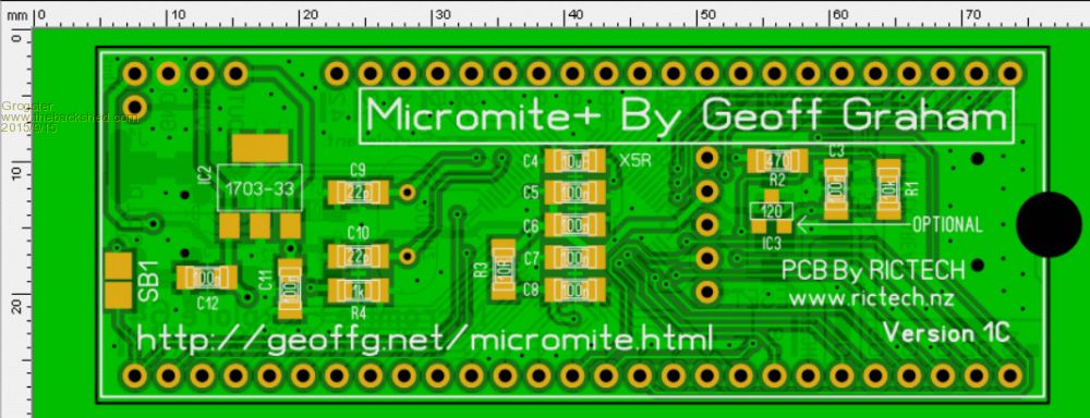
Smoke makes things work. When the smoke gets out, it stops! |
||||
| MicroBlocks Guru Joined: 12/05/2012 Location: ThailandPosts: 2209 |
Looks good. I only have some remarks about the silkscreen, so it is not really important. On the front: MCLR should read #MCLR (Was discussed long time ago in other thread and it is a better way then having a line above the word as it can be misinterpreted. Maybe good to set 'the standard'for uMite use. The pin descriptions of the SD card and t5he USB are under the parts and cannot be seen when mounted. It wouod be nice to have them visible by moving them a bit. This helps when you need to troubleshoot as the pin names are then available. With the SD rotate the numbers so they are in the same orientation as the pin names Rotate X1, D1 90 degrees clockwise. On the bottom: Rotate IC2, C11, R3, R1 90 degrees clockwise. Now i look at it again, i have another thing to ponder. Special reason to have a through hole part for the crystal? It seems it is the only through hole part on the board. If you are going to reflow later it might be nice to have everything in SMD. An SMD version on the bottom will make the tracks a lot shorter and you will have more ground plane under and around the crystal, which is a good thing. It is not super critical that traces are the same length, if you can get close enough it would be nice and rules out another change of a very difficult to find fault. With higher speeds this is more critical. Check the datasheet for a guidance for mounting the crystal. I'll go look now to find the page. edit: Here it is: http://ww1.microchip.com/downloads/en/DeviceDoc/60001185D.pdf page 29. The recommendation is on the same side of the pcb, but that seems to be too difficult now. Maybe a lesson for both of us in the future and that is START with the crystal, then route the rest. Was this a design by committee? Or did it just happen like that.
Microblocks. Build with logic. |
||||
| paceman Guru Joined: 07/10/2011 Location: AustraliaPosts: 1329 |
Like the added component ID's, and since we're still going here 
- the component ID font size could go up a bit - it's pretty tiny. - the "3v3" would look and fit better directly above the "OUT", also then you don't need the 'dash'. Greg |
||||
| The Back Shed's forum code is written, and hosted, in Australia. | © JAQ Software 2026 |
