
|
|
Forum Index : Microcontroller and PC projects : Special "Back Shed" offer on Autotrax DEX
| Author | Message | ||||
bigmik Guru Joined: 20/06/2011 Location: AustraliaPosts: 2981 |
Arghh, Thanks Jean you are right, I looked at the heading on the top of the page rather than the smaller print part names ... Rush job, I am afraid in between doing the work of 2 people at work today.. Unfortunately I cannot update until probably the weekend as I am on the road all day tomorrow. The 64 pinner may also suffer the same problem, Sorry about that... The footprint should be fine though as they are shared across the range.. Regards Mick Mick's uMite Stuff can be found >>> HERE (Kindly hosted by Dontronics) <<< |
||||
| robert.rozee Guru Joined: 31/12/2012 Location: New ZealandPosts: 2541 |
have joined the club, purchased DEX a couple of hours ago. it has taken me this long to find out where to enter the activation key! cheers, rob :-) |
||||
| Justplayin Guru Joined: 31/01/2014 Location: United StatesPosts: 330 |
I was thinking along the lines of a new Mono-Matrix board for the single color matrix LEDs and a Mik-Matrix BackPak. The Mik-Matrix BackPak would be a small board to plug directly onto the back first Mik-Matrix (or Mono-Matrix) module. With connections for a DS3231 clock module, a 18B20 and a DHT22 module. I think the whole thing would hide nicely behind a couple of matrix modules. I'm getting tired of the rats nest of dupont wires holding my current matrix test setups together. 
--Curtis I am not a Mad Scientist... It makes me happy inventing new ways to take over the world!! |
||||
| Justplayin Guru Joined: 31/01/2014 Location: United StatesPosts: 330 |
Wow, I haven't tried using AutoTRAX in a long while and had forgotten how often Iliya releases updates. I loaded the new version this afternoon and few hours later it had already had two updates. --Curtis I am not a Mad Scientist... It makes me happy inventing new ways to take over the world!! |
||||
| bigmik Guru Joined: 20/06/2011 Location: AustraliaPosts: 2981 |
@Justplayin, Yes! That is one thing I must say I am not super happy about.. There is on average 1 update per day. The real issue is that you do not know what is in the update till you download it.. On my broadband it isnt generally a problem but if you had limited bandwidth it could be something to watch out for. You can of course turn updates OFF and update every week or month as you see fit.. Mick Mick's uMite Stuff can be found >>> HERE (Kindly hosted by Dontronics) <<< |
||||
| bigmik Guru Joined: 20/06/2011 Location: AustraliaPosts: 2981 |
Hi All, Here are all (hopefully) Corrected '470 parts.. I might redo the names later to reflect Micromite names but these are the standard MChip names. Any problems let me know. 2016-04-29_070356_PIC32MX470F512.zip Kind Regards, Mick Mick's uMite Stuff can be found >>> HERE (Kindly hosted by Dontronics) <<< |
||||
| MicroBlocks Guru Joined: 12/05/2012 Location: ThailandPosts: 2209 |
Mick, i am also making some (uMite) parts at the moment. I have a different style then you so that will add to the diversity. :) Might it be a good idea to open a specific topic for that? Microblocks. Build with logic. |
||||
| bigmik Guru Joined: 20/06/2011 Location: AustraliaPosts: 2981 |
@Microblocks, That will be great,,,, Who said I have style?. Mick   Mick's uMite Stuff can be found >>> HERE (Kindly hosted by Dontronics) <<< |
||||
| JohnL Senior Member Joined: 10/01/2014 Location: SeychellesPosts: 128 |
Autotrax Dex didn't exactly have a good review and run on EEVBlog. But, most criticism came from professional experienced PCB designers. Long thread 18 pages, there are other threads/posts on EEVblog do a search if interested. http://www.eevblog.com/forum/chat/free-unlimited-version-of-autotrax-pcb-design-software/ |
||||
| bigmik Guru Joined: 20/06/2011 Location: AustraliaPosts: 2981 |
@JohnL, No it didn't, well at least by some people. If you actually read the comments (many many MANY hours of reading for the full thread) you will see quite a few people actually liking DEX, it was unfortunate that in the world of the internet some people like to elevate themselves to show how great and wonderful they are and if they are strong willed they will not see reason and only shout all the more louder. The bottom line is it was being compared to programs costing many $1000 such as Altium which is not really a fair Comparison, I can like my $30,000 Volkswagon and find it does everything that I want but if you compare it to an $800,000 Bently will it compare favourably?. Of course not.. Did they compare Eagle and Diptrace in the same way as they did Autotrax? I doubt it. (in truth they may have but I am not aware of it). That thread you refer to was really a clash of heads between several strongly opinionated people (No I was NOT one of them, I participated but I left the arguing to others) that really got out of hand, there was abuse being thrown both ways. Whilst some of the main protagonist's comments were quite reasonable, Iliya bent over backwards to assist him but he then jumped and criticised something else.. I really think that he did not really want to be constructive and was really hell bent on proving that a $99 product was inferior to a $8,000 one from somewhere else. In all honestly, If you found a bug of minor to medium importance, how long do you think it would take for Altium to release a fix? Iliya usually responds to bug fixes overnight or the next day with these fixes. Even with suggestions he is very obliging. If you are stuck with not knowing how to do something he will respond with an answer. That kind of service is better than most other products of any kind available on line.. Autotrax DEX has improved considerably since that forum started and in reality is not the same product today as it was then. Curtis mention he had 3 updates in a few hours, whilst that is unusual it shows the extend that the program mmorphs. In 12 months time DEX will be different again. To finish of my `rant' (no I really want to be honest not ranting). There are MANY people around the world who use and love Autotrax DEX, Does it do everything that every other similar product does? No! but I believe that for the price of $39 you really should not complain about it too loudly.. It performs well above its price range. Kind Regards, Mick Mick's uMite Stuff can be found >>> HERE (Kindly hosted by Dontronics) <<< |
||||
| bigmik Guru Joined: 20/06/2011 Location: AustraliaPosts: 2981 |
Hi All, As Mentioned, DEX is improving the 3D visualisation at the moment and I just wanted to show a couple of examples of the effect, hoefully TBS wont resize these images too small. The latest effect is to add a `weave' to the fibreglass PCB so that it looks a bit more realistic. (that probably wont be able to be seen in the reduced size of the screen shots but I can follow up with a close up if anyone is interested. 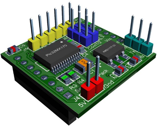
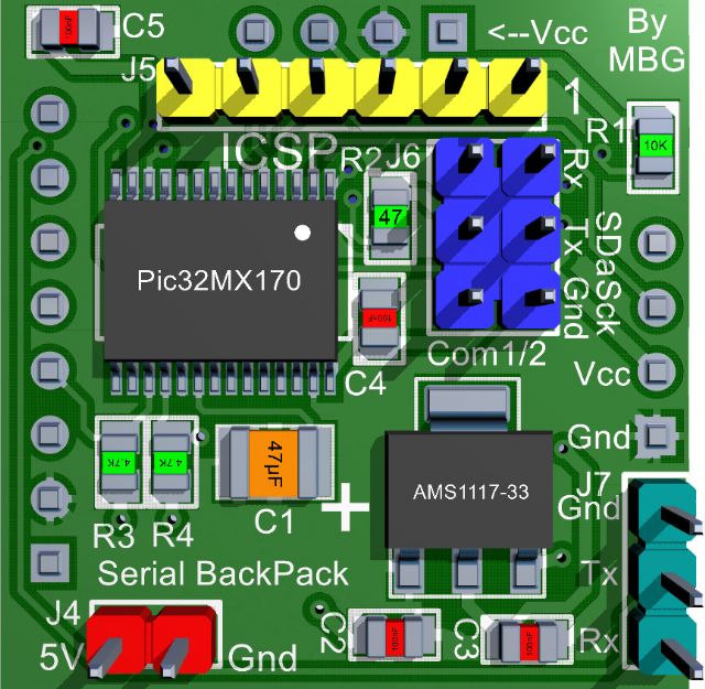
Kind Regards, Mick EDIT**** Yes TBS reduced the size so the weave couldnt be seen. Here is a close up view. 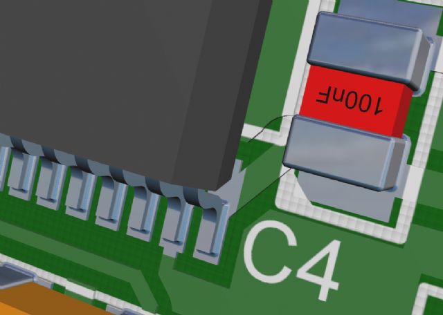
Mik Mick's uMite Stuff can be found >>> HERE (Kindly hosted by Dontronics) <<< |
||||
| MicroBlocks Guru Joined: 12/05/2012 Location: ThailandPosts: 2209 |
The 3D visualization actually was the thing that convinced me. I like that a component is not only a footprint and a 3d model. Here it is actually a parametric model with parametric feet. This gives the most realistic representation with the least amount of data. Very smart. There is even solder on the pins. But what really makes a difference is that each component can have a color. In your example the headers and resistors is a great use. My biggest wish is colored traces, but i can understand that is more a 'false color' 3D but great for documenting a project. It would save a huge amount of coloring by hand. I am not convinced that having the schematic and pcb being one single entity is the best thing. More working with it will make that clear as i am still finding my way around. One thing that bothered me was that I deleted some traces on the pcb that directly removed those traces from the schematic. I think it would be better to change the behavior in the PCB layout to 'unroute' a trace when hitting the delete key. A few small other things like switching between keyboard and mouse when a right click would be much faster to do. Especially 'copy' 'paste' which is either a keystroke or a long travel with the mouse pointer. I am collecting those 'productivity enhancing' things i miss and will suggest them. Microblocks. Build with logic. |
||||
| bigmik Guru Joined: 20/06/2011 Location: AustraliaPosts: 2981 |
Hi Jean, All, Personally it is the ONLY way IMHO, Even the later PROTEL99SE did it that way.. It makes sense to only have one file for your project not 2 (or 3). The project project file can even have PDFs and other documents added (datasheets etc) to keep everything together and in the one place.. To me that is perfect.. If you have a schematic and PCB separate and you do several edits, come back years later how do you know for sure that the particular schematic belongs to that version of PCB?.. At least being in the same file you know they belong together. That is part of the `learning curve' what you actually wanted to do was UNROUTE a tack/segment/NET etc to do that in the PCB select the track/Segment/NET then right click and select UNROUTE Track/NET/Segment(s).. That will keep the Schematic unchanged... YES!! I fell for that one too.. Iliya is always open to suggestions.. Use the DEX forum to make them. I really don't do much keyboard stuff it is almost all mouse work. Have you done a sample board yourself yet? Kind Regards, Mick Mick's uMite Stuff can be found >>> HERE (Kindly hosted by Dontronics) <<< |
||||
| MicroBlocks Guru Joined: 12/05/2012 Location: ThailandPosts: 2209 |
Yes, i am busy remaking a 'MicroBlocks' in DEX, and i am getting more used to it. I 'solved' the deleting traces in PCB by changing the short cut keys definitions. I now have 'unroute selected segments' under the delete key. And the 'delete selected' has now CTRL+DEL key combination. At least it now is not too easy to disrupt a schematic. Another thing i tried was to 'lock' the schematic. For me 'lock' means not able to change it. But even then deleting a trace in pcb deletes the wire in the schematics. My 'flow' is to first finalize a schematic, and then make 1-2-3 different PCB's and choose the best one (or two!). Different placements can drastically reduce routing problems and having that ability is at least for me very important. Often when i get stuck routing, i copy the PCB, reference it to the same schematic, move some parts around and then try to finish the routing. When the results are worse i revert to first PCB and make a new copy, move some parts around differently and try again. This can be spanned over several days, the need for separate files is then necessary. Iterating like that save lots of time and produces for me the smallest pcb's possible, which is one of my goals. The 'one file' for everything does not allow that, and forces me to also copy the schematic, which are then two entities that i have to maintain. Once change in a schematic forces a change in another, resulting in more work and more chances for mistakes. Another is that with parts the footprint is attached to a 'symbol'. Changing a 1201 capacitor to a 805 capacitor is deleting the part and placing a new one and drawing the wires again. In Diptrace i select 'footprint' and change it directly. Or i replace part which keeps the wires connected. Much easier and something i will also suggest. I work with schematics and pcb for hours a day, simplicity and speed are important and if an error is made it should not propagate from part, to schematic to pcb or the other way around. Again for me the schematic is 'MASTER OF EVERYTHING' and the one thing i have to keep absolutely correct. Everything else is referenced and checked against that. I have the feeling DEX complicates that part by integrating and live referencing everything. I will see, i give it a few more weeks. Microblocks. Build with logic. |
||||
| bigmik Guru Joined: 20/06/2011 Location: AustraliaPosts: 2981 |
@MB, To change the shape/type of part, eg. from THP to SMD all you need to do is select PART BUILDER then click on the part in question and change it to what type you want.. All very straight forward and easy.. The wires in schematic will still be ok.. In your case from 1206 to 0805 is the same as above no tracks will into ute although they will move to still connect to the new position of the pads which might need re positioning. Mick Mick's uMite Stuff can be found >>> HERE (Kindly hosted by Dontronics) <<< |
||||
| MicroBlocks Guru Joined: 12/05/2012 Location: ThailandPosts: 2209 |
Mick, That comes close. How do you do that when you want to change 12 of them. :) What i miss a bit is discoverability. The right click is very underused and does not really show options useable in the current context. If rightclicking on a part it shows Zoom and pan options, that is not very usefull. If instead it would show 'part builder' and other relevant options (on the top) it would make it so much easier. I feel like i am on a treasure hunt. And in software that is undesireable. I am a programmer myself, so i was/am guilty of that too, as such it is not 'Diptrace is better' but once i get a few more of these 'smoothing out the user interface' things i will make a suggestion to the developer. I just don't want to send a 'complaint'. I better get more familiar with it and then do some suggestions with have some solid reasoning behind it. Microblocks. Build with logic. |
||||
| bigmik Guru Joined: 20/06/2011 Location: AustraliaPosts: 2981 |
@MB, If I had 12 of them I would just do them, pin the part builder to the side panel so it always is there, resized in width to suit your screen, then do them each in turn, it is only click on part, select type you want, then click the next part and so on... I reckon less than 5 minutes to do all 12. I use right click all the time, I rarely use any key strokes.. I dock my library, design rules, part builder and properties on the left hand side so they are tabs on the side panel, click in one and you will see a thumbtack (gee I hate that name for a drawing pin) click it and it pops out and stays out. There is also a nice option for properties under the panels tab in the top bar area called pop up, then every time you click on something it pops up a little menu, it can get annoying if on all the time but to do many changes to thing like text, track widths etc it's great,.. Anyway, I am far from an expert in all the things that Dex can do and that is where the support forum can help you.. You can ask questions and offer suggested improvements etc.. If there are bugs you find, there is a bug reporter in the help menu.. Don't forget there are around 100 video clips on the Kov.com site that can be quite useful as well. Mick Mick's uMite Stuff can be found >>> HERE (Kindly hosted by Dontronics) <<< |
||||
| MicroBlocks Guru Joined: 12/05/2012 Location: ThailandPosts: 2209 |
Well, after a whole day i have to conclude that this product is not ready. Too many bugs in all major parts, building parts looses pin, descriptions, pin names, schematics loose wires, PCB has a disappearing board outline, 3D is rendering the parts far away from the board, etc, etc. I think i will revisit it in a few months as this costs way to much time, especially redoing stuff again and again. I got the most recent update, but i have the feeling that the older version 7 is much more stable. It has a lot of potential, but as said it is far from ready. I am not willing to be a product tester and file bug reports. The biggest problem i have now with the product is 'trust'. Do i trust it to be able to design something and send it for manufacturing. With all the hiccups i have to say i do not. One thing that i do not wish to do is manually check everything. So it is back to Diptrace for me, as that has not let me down at all. Microblocks. Build with logic. |
||||
| bigmik Guru Joined: 20/06/2011 Location: AustraliaPosts: 2981 |
Hi MicroBlocks, Sorry but which version are you using? I am at work and my laptop is updating now from 8.01.22GL to 8.01.29GL Some of your issues I have NEVER seen. I have never seen the PCB outline disappear, Parts that I have used have never rendered the 3D `off board'. I have never seen PINs or PIN names disappear.. I have seen wires in the schematic disappear when I have inadvertently DELTED a track instead of UNROUTING a track.. That took a bit of getting used to initially. I can assure you that if DEX did, (as you say it does for you), for me I doubt I would have persisted as long as I have. But consider that I have made many perfectly functional boards with DEX and any issues I had was my fault and not DEX's I would have come `a cropper' (Aussie for been in trouble) before now.. Maybe a brief description of `my' methodology of creating a board is in order.. as I suspect you are trying to force DEX to do things in the method that you are used to with Diptrace. I start with the schematic, first I load my parts from my library and move them around where I would like them to be positioned.. Then I link the NETs (wires) to get them connected.. After I am happy that the schematic is as I want I then look at the PCB. In the PCB DEX starts with a default size PCB and all of the component footprints around the outside of the board. I then resize the board to the desired target size I am looking for. I then drag the parts that need to be in set positions (and set which side they should be on) onto the PCB area (The NETs will start looking cluttered at this stage so you can turn these OFF in the View tab in the tool bar). Once the positions are in place I then right click on these components and LOCK them so they cannot be moved without unlocking first. When the parts that are in set positions are done then bring in the other parts onto the PCB into positions you think they should be.. Then turn on the NETs and look at the Nets-nest and rotate/move if you can see that it might make routing easier. Then I right click on NETs that I want wider (Vcc/Gnn/5V etc) and using the properties panel set the widths. I then select AUTOROUTE and watch ELECTRA do its thing.. when finished you will generally find most if not all tracks are routed, there will be the odd funny bend that you can easilly edit out but generally it does a fairly good job. I then spend a lot of time manually re-routing tracks to try to minimise Vias and moves parallel traces further apart if I can but that is just me you could leave all alone at this stage, especially if you have a larger PCB area and the parts spread out (I try to squash my boards down to make them as small as practical and that does take a fair bit of effort). I use the DESIGN rule checker to check for board errors, this does a fantastic job and finds things you might have overlooked. (Set the rules first -- fairly self explanatory.) After I am happy with the ROUTING (electra/manual) I then click the check box at the bottom of the Layers panel to PCB FIlled and make the top Silkscreen visible and the current layer and edit the silk screen overlay to your desire. You might wish to rotate/resize Component designators or resize the silkscreens to suit your requirements. After the DRC passes to your satisfaction and the silkscreen looks good I then place a copper pour on both sides of the PCB, In properties select "resize to board" and tie it to a NET (I use GND) as desired.. Some people use Vcc on the top and GND on the bottom but I dont really like that but it is personal tastes. Then when the board looks OK I tell DEX (in the tools menu) to GENERATE the gerber files and then generate the drill file. That is it in a nut shell.. Watching some of the many videos on KOV.COM will fill in the blanks from my babblings.. In any case I am sorry if it doesnt suit you, I am surprised you had so many issues and I wish I could just pop on over and have a look at your setup.. As I have said before there is a bug reporter if you have indeed found a bug and the forum is quite active and you will generally get your answers overnight if you are stuck. I am always ready to assist you or anyone if I can. Regards, Mick Mick's uMite Stuff can be found >>> HERE (Kindly hosted by Dontronics) <<< |
||||
| bigmik Guru Joined: 20/06/2011 Location: AustraliaPosts: 2981 |
Hi All, Iliya has been reading this thread and responded with this answer regarding separate SCHEMATIC and PCB files and Track Highlighting. Regards, Mick QUOTE Iliya.. ___________ Doing 2 different PCBs with one schematic in a single design is full of problems. The main one is that often the pin numbers on packages are often different for different package types. What if a different PCB combined elements into 1 e.g. resistor arrays. DEX has a one to one mapping of symbols/footprints so select a symbol selects a footprint. Same with schematic wires to tracks. The complexity and risk of software bugs would go through the roof! I could do this but to be quite honest it’s not worth it. Other programs might handle it with users clicking forward/reverse ‘annotation’. These are not real-time links. I think often they have problems. Reverse annotate a PCB to a schematics, what about the other PCBs made from the same schematics. As for colored tracks matching colored schematics wires; what about layer color? In DEX select a wire the PCB net and all its tracks get selected. Same the other way. Try the route panel to select named/unnamed nodes/nets. Regards Iliya Kovac 
EDIT**** TBS reduced the image size to be almost unreadable.. Here is a ZIP with the Image file full size. 2016-05-01_023303_Iliya.zip Regards, Mick Mick's uMite Stuff can be found >>> HERE (Kindly hosted by Dontronics) <<< |
||||
| The Back Shed's forum code is written, and hosted, in Australia. | © JAQ Software 2026 |
