
|
|
Forum Index : Microcontroller and PC projects : Special "Back Shed" offer on Autotrax DEX
| Author | Message | ||||
| robert.rozee Guru Joined: 31/12/2012 Location: New ZealandPosts: 2541 |
i think the 2 or more boards from a single schematic question could be mostly addressed by adding the following two small features: 1. in the schematic editor provide a "read only" switch, that can be set on to lock out editing of the schematic. so once you have your design complete/perfected (as much as any design ever is) you can be assured that whatever you do in the board editor, the schematic remains untouched. 2. provide a means (if it is not already there) to quickly erase the board portion of a project, without touching the schematic. using a copy of your working project, you can then create an alternative board layout. before doing this (but after erasing the original board) you would want to go over the schematic and update any component packages and pin numbers that need changing for the new board. the above two would get you 99% there. the final step, if one really wanted it, would be a 3rd-party program to extract the netlist from two different DEX projects, and produce a sensible 'difference file' showing what components/pins have changed from one schematic to the other. cheers, rob :-) |
||||
| MicroBlocks Guru Joined: 12/05/2012 Location: ThailandPosts: 2209 |
@Mick, I have EXACTLY the same workflow! I tried to get to the bottom of the error and i hope i have found it. I made a part, a PIC16F1455. 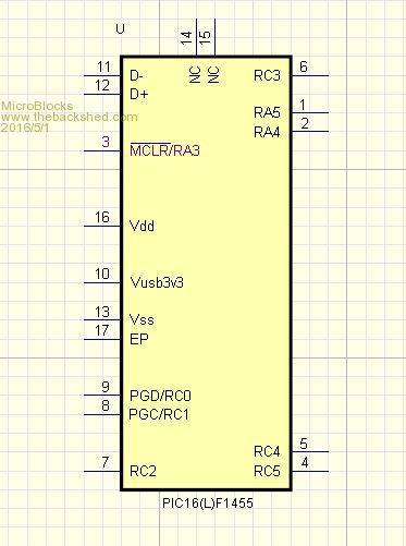
Placed it on the schematic with a header, capacitor and a Vcc terminal. Draw some lines. 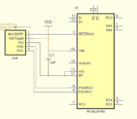
Noticed a less optimal placement of a pin. Edited the part. Then in schematic selected it , then refreshed from library. At that moment my PCB is basically destroyed. 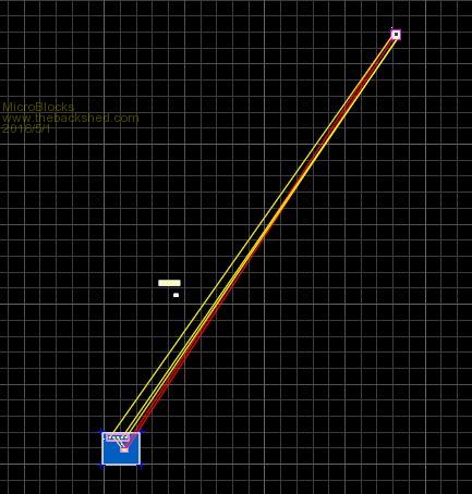
Even some phantom 'parts' appeared. 
The board boundaries are also gone but reappear after a click, so that is not really a big bug, more a UI glitch. At first i thought it was caused by me accidentally dragging the footprint 'placement point' (WHICH IS AN ABSOLUTE NO NO!!!! What is the point of a library if part footprint is not absolutely locked!) but after discarding everything and start over (for the fifth time) i ruled that out. About trace colours. Layer colors are a nuisance when having more then a few layers. Trace colors however can easily show where important traces are, especially like power lines and important signals like SPI,I2C etc. I guess for analog circuits there would be equally important traces to pay extra attention to. If using layer colors and trace colors you would obviously not use the same colors. It is a productivity improvement tool. Coloring parts in 3D is very useful but compared to colored traces it is just a toy. Wrong priorities, but i understand the reason. 3D sell, coloured traces is ... meh... nothing special only to find out that it can't be done. Microblocks. Build with logic. |
||||
bigmik Guru Joined: 20/06/2011 Location: AustraliaPosts: 2981 |
Hi Jean, I have created many parts and I have not seen the likes of that. I admit I did have a similar situation occur once where I selected show all and the PCB was a tiny little thing in the centre of the screen. It turned out that for some reason I had a Component text appear miles away from the component.. It only occurred to me the once many months ago.. When you created your part did you use the part creator? See this image in the LIBRARY tab. It loads a part creation wizard and I have never sen it do what you have shown there. 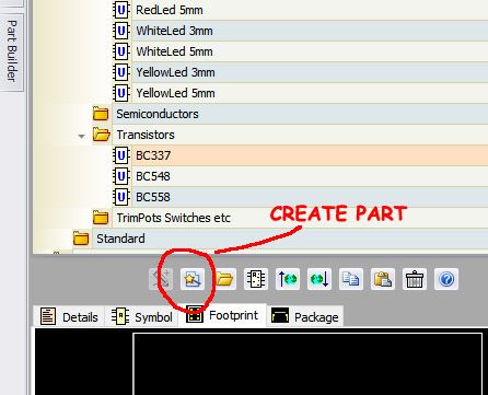
Kind Regards, Mick Mick's uMite Stuff can be found >>> HERE (Kindly hosted by Dontronics) <<< |
||||
| WhiteWizzard Guru Joined: 05/04/2013 Location: United KingdomPosts: 2991 |
Just my luck - does anyone know if the offer has been extended beyond 30th April (without me going through all these posts?) I am in need of a new PCB package as one product I was needing to create has hit my 10cmx8cm limit for Eagle. |
||||
| bigmik Guru Joined: 20/06/2011 Location: AustraliaPosts: 2981 |
Hi WhiteWizard, All, I sent Iliya an email and he has responded with an extension for another week.. The original link on the first page should now be working again.. Offer expires May 7th. Regards, Mick Mick's uMite Stuff can be found >>> HERE (Kindly hosted by Dontronics) <<< |
||||
| MicroBlocks Guru Joined: 12/05/2012 Location: ThailandPosts: 2209 |
Mick, yes i use the part builder. made a QFN by changing a few parameters. (That part is great timesaver). Little bit bummed that i do not get it to work. Thrown out the part, deinstalled dex, erased all directories and installed everything fresh. Maybe i have done something that got stuck. Will update my progress on that. Microblocks. Build with logic. |
||||
plover Guru Joined: 18/04/2013 Location: AustraliaPosts: 306 |
I am following as time allows this thread with interest, I am tempted rush in and install my copy but I have already overstretched or overestimated my job list, I will have to stay on the sideline and watch. MicroBlocks your next learning project, I assume they are small, before tossing it out what about attaching a copy to this thread? Whoever is learning as well could then pick it up and play with it and report findings as well? I am assuming a project is not monster file sizes. |
||||
| skylight Newbie Joined: 10/01/2016 Location: United KingdomPosts: 23 |
Thanks bigmik for setting up this offer |
||||
| bigmik Guru Joined: 20/06/2011 Location: AustraliaPosts: 2981 |
Hi Skylight, All, Whilst I did ask Iliya, to make an offer for TBS Members, that is all I have done.. I know there are quite a few people on TBS who use DEX and, presumably, working OK with it.. I myself have used it now for 2 years and quite like it. Yes it took a while to shake PROTEL99se methods from my head, in my case I feel it was tough because the PCB screen (and the schematic as well) was so close to looking like PROTEL that the `deep recesses' of my brain thought I was using PROTEL and I had to re-learn how to do everything from scratch. Sort of like trying to write Left handed when you have been using your right hand all your life.. YOU CAN DO IT you just need to use it the way it was intended.. I intend to duplicate MicroBlocks circuit later today to see if there is some weird problem he has encountered. @MB, I am wondering if it is because you are a `keyboard' user that something didn't work as you expected.. You stated you were setting up keyboard shortcuts and things.. I swear I hardly touch the keyboard except for entering in TEXT and navigating left/right/up/down.. I even tend to use the mouse to change track widths by rolling the mouse wheel to change the sizes.. I wonder if this is the root cause of your problem.. I feel that DEX is a MOUSE product not a keyboard one (although I am sure it can be used via the keyboard). Anyway, I think Thanks belongs to Iliya, NOT me.. He has made the offer I just invited him to make it. Kind Regards, Mick Mick's uMite Stuff can be found >>> HERE (Kindly hosted by Dontronics) <<< |
||||
| bigmik Guru Joined: 20/06/2011 Location: AustraliaPosts: 2981 |
Hi MicroBlocks, I tried your demo from scratch and didn't have any issue like you experienced. Here is my interpretation of what you tried to do. I created the part from scratch using the Part editor (one Issue I will mention at the end of this message) 2016-05-02_013725_PIC16LF1455.zip Then I drew the schematic with a 1nf cap (0805 footprint) with a 5x1 Male header (one of my earlier parts in my libraries) 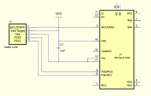
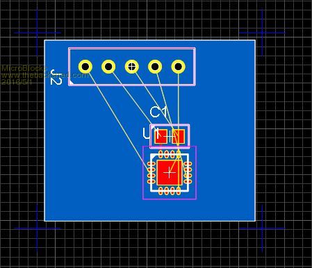
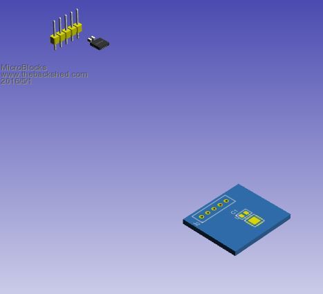
Then I Re-sized the PCB to be of a suitable size for the parts and routed with electra. I changed 1 track from the bottom layer to the top to eliminate a via that wasnt necessary (My anal-ness there) 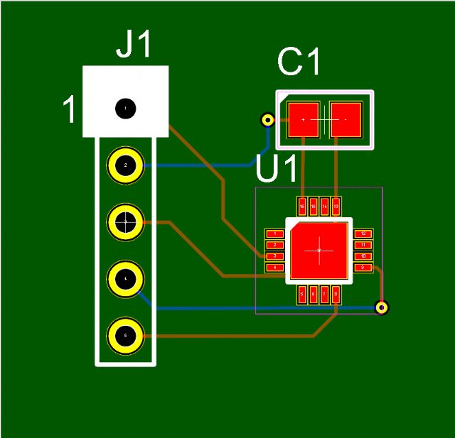
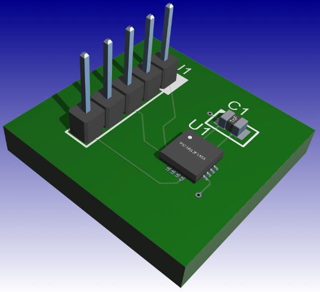
Here is the project file for your interest /2016-05-02_014113_MicroBlocks.zip">2016-05-02_014113_MicroBlocks.zip Now I mentioned earlier that there was one issue with part creation (using the part builder wizard).. After creating the part as a 4 x 4 QFN (yes my image is TQFP as there wasn't a default QFN pack in part builder) I rearranged the image in the schematic to reflect your layout I then realised you had a pin 17 which I gather was the metal tab underneath the Chip itself, so I went to the PCB and added a PAD (#17), and resized the silk screen to clear the pad and resized to 2.5mm square (as per datasheet) then when I went back to the schematic I had it had reverted to the square (ish) shape the part builder created.. Damn that cost me 2 minutes of my life to re-do 
I think that is a minor bug that I will report to Iliya but over all I didnt have any issues with your example.. I hope when you re-install that everything works as expected. Kind Regards, Mick Mick's uMite Stuff can be found >>> HERE (Kindly hosted by Dontronics) <<< |
||||
| bigmik Guru Joined: 20/06/2011 Location: AustraliaPosts: 2981 |
Hi All, Iliya has just posted a `roadmap ' of things he will be prioritising in the SUMMER (well it getting new WINTER over here but I assume he means UK SUMMER) 1. fix bugs 2. parts manual with loads of videos. 3. docs 4. new router No doubt with the new improvements recently done with the 3D he is going to add better support for `parametric' parts, these are auto generated by DEX and are much smaller in bytes than importing 3D models. Kind Regards, Mick Mick's uMite Stuff can be found >>> HERE (Kindly hosted by Dontronics) <<< |
||||
| MicroBlocks Guru Joined: 12/05/2012 Location: ThailandPosts: 2209 |
Mick, the link is not working. I made the 'QFN' the same as you did. Selected a TQFP and then selected the leadless checkbox under 'Parameters'. After a night sleep and trying to think what the exact moment was that things went wrong there are two possibilities. One is redefing the Del shortcut which might have strange behavious or (and i suspect this highly now) the update to 8.01.24. ps. Thanks for trying out and show that it works. Must be something wrong at my side. I have done a reinstall and checked all my drivers. Edit: I FOUND THE PROBLEM!! I recreated everything and it works fine now. Loading the previously made part this is the difference: Problematic part: 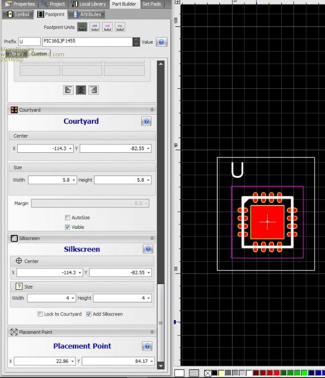
Good part: 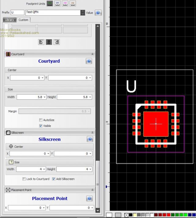
Visually they are both exactly the same. However in the parameters the center X and Y coordinates for Prefix, Courtyard,Silkscreen and Placement point are not from the center of the part in the problematic one. I was also unable to fix the problematic one by changing those values, i had to redraw/generate the part to get the right center. Now the question is how the #$@ did that happen! Microblocks. Build with logic. |
||||
| bigmik Guru Joined: 20/06/2011 Location: AustraliaPosts: 2981 |
Hi MicroBlocks, Which Link? The Offer link is up and working as far as I can see. Autotrax DEX Special OFFER Ahaa!! 2 years with DEX and taught something by someone who has used it 2 minutes..  
Thanks Jean, I never knew that.. Boy do I feel a fool. 
I really suspect it was your re-defining the keys.. I fear that you are trying to force DEX to work the way that you are used to with DipTrace rather than using DEX the way it was designed.. Anyway I am keen to hear how you go with another shot. Not a problem Jean, That is what this forum is all about... Asking for assistance/Advice and offering Assistance/Advice. Kind Regards, Mick Mick's uMite Stuff can be found >>> HERE (Kindly hosted by Dontronics) <<< |
||||
| MicroBlocks Guru Joined: 12/05/2012 Location: ThailandPosts: 2209 |
Mick i just edited my post while you were writing yours! I found the problem! Microblocks. Build with logic. |
||||
| HankR Senior Member Joined: 02/01/2015 Location: United StatesPosts: 209 |
Mick, Check your PM. Hank |
||||
| bigmik Guru Joined: 20/06/2011 Location: AustraliaPosts: 2981 |
@MB, Great news.. I don't understand how that happened but why could you not edit the centres and bring everything back in line? @Hank, Thank you I do not know why the project file I uploaded didnt work (that is a TBS thing..) Anyway here it is again, Note it has the TQFP package for 3D instead of the QFN (big deal) but as Jean rightly pointed out a single click under the part builder on "leadless" (i wonder why he didnt chose the term "LEGLESS" ) does the trick.
Sample MB mini-Project 2016-05-02_044850_MicroBlocks.zip Kind Regards, Mick Mick's uMite Stuff can be found >>> HERE (Kindly hosted by Dontronics) <<< |
||||
| MicroBlocks Guru Joined: 12/05/2012 Location: ThailandPosts: 2209 |
Could not fix it because the numbers for the center did not make sense at all. All the centers in the correct part are 0,0. In the problem part they are different while the visual representation is correct, which would suggest that there are two sets of numbers or two sets of 'origins'. .... some time passes ....... Yep, it is the PCB that is in the 'Part' that has an origin on the left/bottom. The center of the part then changes to a coordinated calculated from that point. Resetting the center of the PCB in the footprint of the part to 0,0 fixes the problem. Now the question is, what is a PCB board doing in a library part? Microblocks. Build with logic. |
||||
| bigmik Guru Joined: 20/06/2011 Location: AustraliaPosts: 2981 |
@MB, The PCB is not actually IN the part it is just a representation for the 3D to give some indication of how it would look in a PCB design. I also noticed you had rounded pads in your original design, was that intentional? Mick Mick's uMite Stuff can be found >>> HERE (Kindly hosted by Dontronics) <<< |
||||
| MicroBlocks Guru Joined: 12/05/2012 Location: ThailandPosts: 2209 |
Yes it is IN the part and will act as an origin somehow when you resize it. You can see the borders of in in footprint. In the properties panel there is a 'Set origin', once pressed all the coordinates are reference from the lower left corner. I think it would have been better to have no PCB representation at all in the 'footprint' as it is not part of a Part. The rounded pads are from the recommended footprint in the datasheet. My 'TestQFN' i did not do it, but after changing it, it still works fine. The culprit is i know now with 100% certainty the lower left origin of the PCB as it is repeatable. Having pads that have rounded corners are very useful when routing gets tight. The square ones take a lot more room as the corners are sharp and prevent traces from being closer to the pad. Microblocks. Build with logic. |
||||
| bigmik Guru Joined: 20/06/2011 Location: AustraliaPosts: 2981 |
@MB, When I say not IN the part, I mean that when you place the part onto your design the PCB will NOT be seen as an extra to the Design's PCB.. so you wouldnt see your design with all these little `pcb's sitting on top.. I agree though, that the `pcb' that you see in the part should not ever be moved from the centre of the part itself.. makes no sense to allow that and can only cause some grief if it gets shifted. Kind Regards, Mick Mick's uMite Stuff can be found >>> HERE (Kindly hosted by Dontronics) <<< |
||||
| The Back Shed's forum code is written, and hosted, in Australia. | © JAQ Software 2026 |
