
|
|
Forum Index : Microcontroller and PC projects : simplest 32MX150 ICSP
| Author | Message | ||||
| MOBI Guru Joined: 02/12/2012 Location: AustraliaPosts: 819 |
Hi, methinks there is more to programming a pic32 than MCHP let on - unless there is something I'm continually overlooking. Is there any one game enough to also tackle the MicroChip documentation? I've wired up two pic32 chips - the top one as a micromite and the other as the target chip to be programmed. For anyone game enough, the connections are simple enough and are listed at the beginning of the code. I would like to be able to get this working (if it is indeed possible) just using the MicroChip documentation - which is a challenge in itself. The code so far should determine the status of the target chip, i.e it is ready to accept programming commands. The pdf of the pic32 programming instructions is on the previous post to google and download. 2014-05-16_074429_picprog.zip 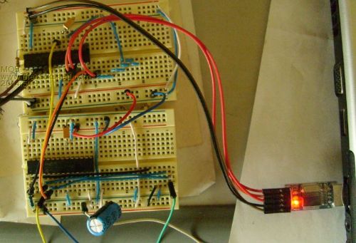
David M. |
||||
| WhiteWizzard Guru Joined: 05/04/2013 Location: United KingdomPosts: 2991 |
Hi Mobi, I am working on this in my 'spare' time to running the website (MicroMite.org). I haven't yet seen your code but I will take a look and pass it by the analyser to see if I can help you. Was making good progress myself but I couldn't find where it was that the PIC32 replied with it's Device ID. If I discover this (maybe from your code) I will be able to progress further. Give me 24hrs and I will try and respond back . . . . WW |
||||
| MOBI Guru Joined: 02/12/2012 Location: AustraliaPosts: 819 |
Hello Wiz, I don't think you will find that from my code. I got to the stage of reading the device status byte which came back blank - so something wrong. Are you trying to use a MicroMite as the programmer? I developed code that is supposed to mimic the pseudo code operations e.g. sendCommand, setMode ,TransferData etc. I think it is in at least one of these that something is wrong. The wife and I are heading off to an outback nature reserve for a working bee on Sunday for a week of conservation work and will be totally out of internet contact. Today/tonight I will have another try using raw bit patterns instead of general purpose calculated data from sub routines. If I can get the "statusVal = XferData (MCHP_STATUS)" to respond, I'll know I'm on my way. David M. |
||||
| Keith W. Senior Member Joined: 09/10/2011 Location: AustraliaPosts: 118 |
Mobi and WhiteWizzard, It is so convoluted to communicate with the chip. 
I have looked briefly at Mobi�s code but must wrestle further with the documentation. If the chip to be programmed contains an MMBasic Autorun program that will for instance continually flash a LED, then when after the sequence to enter ICSP Mode and Mclr goes high, if this has failed then the LED flash program will run. Otherwise you have likely succeeded in entering ICSP Mode? Perhaps to test just this Moby�s program should halt at this point with Mclr high? This test will hopefully show that at least the chip is in ICSP Mode as a very first step, but for me not until tomorrow. Perhaps others have already performed this test. That the serial data should require most sig bit first to enter the Mode and then least sig bit first for commands and with different clock edges hints at the gymnastics required in the protocol. I have still to fully grasp the interleaving of 4 wires to 2 wire data that seems required. I think that we should conform somehow to Figure 6-6 page 15 of DS6001145M. Is this correct? Keith W. |
||||
| MOBI Guru Joined: 02/12/2012 Location: AustraliaPosts: 819 |
Keith, I'm not sure I'm reading you right but here goes. The two wire system as used by say PICKit3 only has a bidirectional PGD (programme data) and out only PGC (clock). In the 4 phase two wire system there are three bits of data namely TDI (data in to the target), TMS ( mode select) and TDO (data out). They are always clocked in the same sequence. The TDI bit is placed on the PGD pin and the clock toggled hi/lo. Then the TMS bit is placed on the PGD pin and clocked in, then a third clock and lastly, the TDO is read out on the PGD pin. That is 4 clock pulses. The sequence is always the same. The TDO is clocked to the PGD pin on the high going clock edge, read by the programmer then the clock is returned to 0. At the fourth clock pulse, the programmer must change its PGD pin to an input. All 2 wire 4 phase functions use the same pattern. To clock in an 8 bit byte would take 32 clock pulses plus any extra for TMS header and footer.. I have stopped the programme at all sorts of places and all seems to be working up to checking the chip status which returns zero. I like the idea of using a pre programmed chip and stopping at mclr hi. I haven't tried that. ================= I tried the blinky led suggestion and it wasn't going into programme mode, so I started (again) to look further. I have said it a million times in the past (ok so I exaggerate) if the software looks like it should work, it usually does and go (out of desperation) to look for hardware faults. I have checked this b.... thing until I am crosseyed and could find nothing wrong. The PGD jumper is orange and the PGCK jumper is yellow and it looks all along that I have had them reversed. (how embarrassing). Anyway, now the led stops blinking and I get a status byte that conforms with what I think it should be. Fingers crossed as I try the next step. WW I'll catch up with you yet. Thanks Keith for the hint. David M. |
||||
| JohnS Guru Joined: 18/11/2011 Location: United KingdomPosts: 4335 |
I'm unclear - what happens on the 3rd clock? Is it all completely async i.e. the timings can be very slow? John |
||||
| MOBI Guru Joined: 02/12/2012 Location: AustraliaPosts: 819 |
The third clock looks like an internal operation I've been doing a bit of timing changing and it doesn't seem to bother things - so far. somewhere earlier in the programming instructions it mentioned that all timing was controlled by the external programmer and was in no way dependent upon internal timers. It is imperative that the 4 clock phases occur in the same format every time but not at the same speed. I am now getting a status register reading but it is not correct and won't allow me to erase the chip. Misreading MCHP documentation? (that wouldn't be a first). 2 steps forward, one step back? Are you having a go at this also? The more the merrier. David M. |
||||
| JohnS Guru Joined: 18/11/2011 Location: United KingdomPosts: 4335 |
Thanks. I'm very interested but don't have the time to do much at the moment. I previously had the impression it was rather hard to do / needed a separate uC (such as PICkit 2/3) and so on. (I bought one and don't object - I've a JTAG thing too - but if another way is possible for PIC32 then it's of interest.) The simpler (cruder) the better, so it can be understood (and then spawn better/faster versions). John |
||||
| WhiteWizzard Guru Joined: 05/04/2013 Location: United KingdomPosts: 2991 |
Several weeks ago I was analysing the data, clock and MCLR signals on an analyser while using a PicKit3 to program a MicroMite. I then wanted to decipher the data sheet while referring to the actual waveforms. There first few stages of comms required (as per data sheet) were indeed observed in real life. Then a status feedback was seen that just did not follow the data sheet. This is where I got to and have been head-scrathing since. I guess that there is missing information from the data sheet. An enquiry with MicroChip returned an unhelpful reference to the data sheet I was already using (which I did tell them I was using). I will see if I can visit their techies sometime soon (I live close to there UK head office) to thrash this one out - just need to triple check my work first before I claim they are 'incomplete' with their data! WW |
||||
| MOBI Guru Joined: 02/12/2012 Location: AustraliaPosts: 819 |
Hi Wiz, I have got to the stage of seeing a status byte but it doesn't match the data sheet. The process goes through to the end of "erase chip" (where I've terminated it). It goes into programming mode (my pre programmed blinking led goes out), goes through the erase steps but as soon as I release mclr, the led blinks again which would suggest that erase has failed. I even put in a loop and repeat status read as per data sheet to no avail. Can you remember what length your 'sendcommand' words were? 5 or 6?. The data sheet implies that the length could be 5 or 6 depending on how you interpret the timing charts. In 8 bit pic days, programmer commands were 6 bits. Might have to get my self a logic analyser - there is only so much one can do with a dual trace cro especially with 'one shot' bit patterns. David M. |
||||
| JTR0701 Regular Member Joined: 10/07/2013 Location: AustraliaPosts: 71 |
The length of the payload command as sent by the SendCommand pseudo op is always 5 bits. You do not need to parameterize this. It is always 5 bits. Edit: Plus header and footer as you have. |
||||
| MOBI Guru Joined: 02/12/2012 Location: AustraliaPosts: 819 |
Thanks, I did suspect as much. The difference between 'send command' and 'xfer data' could lead one to think otherwise. I have changed my code a bit to be definitely '5 bits' rather than variable. It does look a little confusing in the 2 wire format that 5 bits are clocked in one block and then the MSB is clocked in the next block. That would suggest 6 bits?? It does puzzle me that even though the device seems to go into programme mode (led stops blinking) and subsequent commands and transfer data for 'erase device' seem to work and produce a status byte, I can't get it to produce the desired status bits. Have you had experience with what I am trying? David M. |
||||
| JTR0701 Regular Member Joined: 10/07/2013 Location: AustraliaPosts: 71 |
No, The last command bit (bit-5) is sent with TMS = 1. While it is shown as a different block in the prog specs it really is just the 5th bit. The difference and point of confusion is that TMS is raised for the 5th bit. Then the 2-bit footer is sent. Your FOR ... LOOP in SendCommand needs to be set for 4 iterations (TMS= 0.) You then do the 5th bit with TMS = 1. (This accounts for the middle two blocks shown in the specs, figure 6-4) You appear to me to be on the right track with what you have. Yes i have some experience. See my earlier post for what I got working with the 16F1455 and assembler code. |
||||
| Keith W. Senior Member Joined: 09/10/2011 Location: AustraliaPosts: 118 |
Hi Mobi, I think that I have discovered a slight anomaly in your description earlier regarding clocking TDO into the programmer. You stated: - ��.. The sequence is always the same. The TDO is clocked to the PGD pin on the high going clock edge, read by the programmer then the clock is returned to 0�. However referencing the timing diagram in Figure 6-6 XferData 2-Wire (4-Phase) The diagram indicates that the TDO data is placed on the chips PGED pin at about the falling edge of the 3rd clock in the in the 4 clock sequence, to be read by the programmer at about the rising edge of the 4th clock. PGED should be a programmer input not an output before the 3rd clock falls. At the speed that your programmer can operate you are probably not anywhere near to the timing limits anyway, and the set up time is sufficient. Perhaps your reading/transmitting of the data is correct with respect to the clock edges but as you are not obtaining the expected result you might investigate? I am still reading, including Kaikkonen�s program that uses Jtag as it is the only published source that I can find that works. Checking it against the process described in the DS60001145M document looking for variance. And I am learning. JTR0701 has indicated we must look at the fine print carefully in the diagrams. Best of luck. Keith W. |
||||
| MOBI Guru Joined: 02/12/2012 Location: AustraliaPosts: 819 |
That is what I originally had but that might have been before I got the clock and data pins the right way around. I am travelling at the moment and won't have too many opportunities to try out code. I'll have another look at the tdi, tms, tdo Send Command charts and see in respect of jtr and keith comments where I might be misreading the data. I'm just not in a position to try thing with the hardware and most likely I'll be out of internet for about a week after tomorrow. thanks for your help, I'll likely need more yet. David M. |
||||
| Keith W. Senior Member Joined: 09/10/2011 Location: AustraliaPosts: 118 |
Hi Mobi Hope you enjoy your trip. I questioned timing but you are busy and I could not stop thinking. Shown here is my interpretation of the 4 clock sequence by editing your "clock" subroutine. I have noted when TDI, TMS and TDO data is shown active, and the position of the clock edge arrows that I have taken as indicating the latching edges. I assume that due to execution speed the clock high or low times and setup times exceed 40 ns minimum as specified and no additional delay is required. My major changes are to make the Programmers PGED pin an input other than between after the rising edge of the first clock and before the rising edge of the third clock, endeavoring to not have the subject chips output fighting the Programmer output. Perhaps pin(pgd) should be an input unless required otherwise. I am interested in what you think about this timing; hopefully I can soon try it. 'create 4 phase clock and read data out on pgd line clock: Pin(clk)=1 'first clock SetPin pgd,dout 'Programmer PGED output on Pin(pgd)=tdi Pin(clk)=0 'latch tdi into chip Pin(clk)=1 'second clock Pin(pgd)=tms Pin(clk)=0 'latch tms into chip SetPin pgd,din 'as chip tdo active soon Pin(clk)=1 'third clock Pin(clk)=0 'enable chips TDO tdo=Pin(pgd) 'as data was ready after fall of clock 3 Pin(clk)=1 'fourth clock Pin(clk)=0 Return [/Code] Keith W. |
||||
| JTR0701 Regular Member Joined: 10/07/2013 Location: AustraliaPosts: 71 |
Indeed as Keith has identified there is output contention with the Mobi timing for the period the "master" takes to lower the clock and reconfigure the I/O. Given that this is done in an interpreted basic framework, this contention could be several ten's of microseconds - not good. I recommend Keith's method as being correct. I also note that the Pickit firmware (and my own) leaves the PGD line as an input between the primitive four phase bit operations, again as Keith suggested. |
||||
| Keith W. Senior Member Joined: 09/10/2011 Location: AustraliaPosts: 118 |
Geoff, What I am about to suggest is ahead of the current progress regarding programming a chip using MMBasic, but I believe that goal will be achieved soon. In earlier posts it has been highlighted that chip programming using MMBasic will inevitably be slow. The clock routine written about in my post above must run hundreds of thousand times to program the chip. It averages at more than one call per transferred program bit state and is fundamental to communicating between chip and programmer. If this clock routine is found to work could it be converted into an MMBasic Function? It will surely run much faster written in C. Here I have called it Pclock and envisage that it would be called as follows: - Pclock (A, B) That it will return the TDO state, 0 or 1 (or a Bool), A = TDI state and B = TMS state. As A & B are treated as Boolean states, a way of passing these variables to the PCLOCK function that minimizes processing would be helpful, perhaps they could be combined i.e. as 0, 1, 2 or 3, giving all combinations. For speed the PGEC and PGED pins should be fixed that no computation to find them be required within the routine. Access to these pins by MMBasic is still required when programming, to enable Mode commands and to enter ICSB Mode. I think that the core Pclock function would take less than 100 bytes but there is the overhead to call it. The 40 ns hold time specified for programming clock (PGEC) is short so likely no padding is required even at assembler speed. I think that this is a viable method to greatly increase the programming speed without converting everything to C code and may mean that an MMBasic based Programmer is practical. Is this a possibility Geoff? Keith W. |
||||
| JohnS Guru Joined: 18/11/2011 Location: United KingdomPosts: 4335 |
So long as a umite can be programmed in no more than some large time (a day?) people will have a tool that saves buying a PICkit2/3. Anyone doing regular reprogramming will have a threshold of pain where they just buy the PICkit! (I don't mean a day, I suspect.) It would make sense to POKE a reprogrammer written in C (ASM if you must) and run it, really. But first a working one would be a good place to start if a C version was wanted, for example. John |
||||
| MOBI Guru Joined: 02/12/2012 Location: AustraliaPosts: 819 |
Hi all, I think this might be my last night with WWW for a few days but then, we do get some mobile net anomalies in the outback. @keith, the 4 phase clock sequence certainly looks workable. I am not convinced that the data is available on the PGD line at the third clock even though the charts seem to indicate. It is after all just a drawing and MCHP are notoriously inaccurate in their representations. (unless you have already confirmed with a logic analyser). I will give it a go though. Why I am concerned is that MCHP have gone to the trouble of including arrows on their clocks and as all timing is done by the programmer, I would think that they would certainly indicate the edge at which the data in or out is latched. That has certainly been the case in the past with PICF88 based programmers I have made for 8 bit pics and avrs. I don't think any timing using the micromite would be too quick for the PIC32 it being an interpreted language, but worth experimenting with. I think that leaving PGD as an input until required otherwise could be a good idea to avoid having pin polarity clashes - not really sure it can though. I'll plug in my dongle and have a bit of a play with the code, bearing in mind the suggestions made. Don't go getting too far ahead of me whilst I'm AWOL. (just kidding, its a free world) ============== I tried the modified the 4 phase clock routine to that suggested but with the same results as previous. - back to the drawing board. Running out of hair. David M. |
||||
| The Back Shed's forum code is written, and hosted, in Australia. | © JAQ Software 2026 |
