
|
|
Forum Index : Microcontroller and PC projects : Stepper Project
| Author | Message | ||||
| mozzie Guru Joined: 15/06/2020 Location: AustraliaPosts: 400 |
G'day Bryan, Not much work being achieved today, stepper ideas and CNC / surface grinders are too much of a distraction  Stepper System GPIO Usage suggestion GP00 SPARE or PSRAM ENABLE GP01 ENABLE GP02 STP X GP03 DIR X GP04 STP Y GP05 DIR Y GP06 STP Z GP07 DIR Z GP08 SPARE or CONSOLE GP09 SPARE or CONSOLE GP10 STP A or I2C (RTC?) GP11 DIR A or I2C (RTC?) GP12 LCD GP13 LCD GP14 LCD GP15 TCH GP16 SPI GP17 TCH GP18 SPI GP19 SPI GP20 B/L GP21 SD CS GP22 E-STOP GP26 LIMIT X GP27 LIMIT Y GP28 LIMIT Z I think this gives us a bit of flexibility depending on if we want SD Card / RTC / USB firmware, what do you think? I would like the option to use the USB firmware because I have a couple of wireless numeric keyboards on the way, if they work with the PicoMite USB firmware it allows direct input of numeric values and jogging of axis. Now back to work.... Regards, Lyle. EDIT: I think our posts overlapped Edited 2026-05-07 14:00 by mozzie |
||||
Bryan1 Guru Joined: 22/02/2006 Location: AustraliaPosts: 2136 |
Ok mate I printed out another pico 2 image and I'll go with your pin assignments  Now I found one of my old I2C RTC's which has a DS1307 RTC onboard, the battery measured 2.95 volts and they have been sitting for about 10 years So yes a RTC is a good idea as we do have the in/out pins for it Also in my stash is an old 3D print head which I got back in the day when 3D printers first came out so that is another project for the future. |
||||
| Bryan1 Guru Joined: 22/02/2006 Location: AustraliaPosts: 2136 |
Just having a play in Sprint Layout and I had to make a macros for the pico 2 footprint then got do the first draft, still got the power to sort out and it will fit on a 100x100 board too 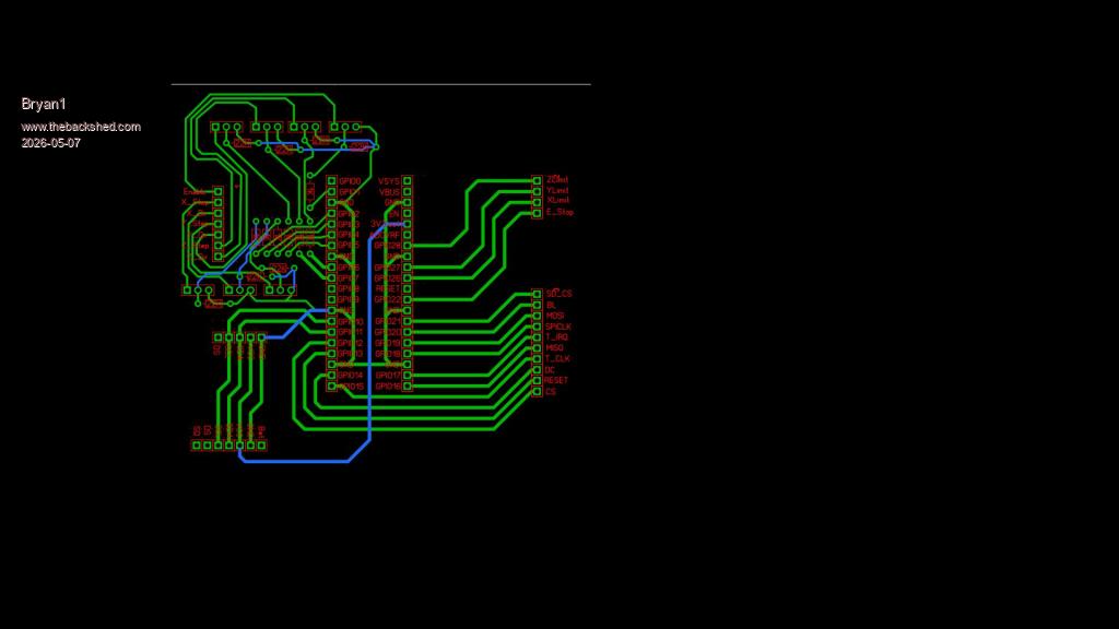 Now this is done with Lyles suggestion of the pin layout, just tested my old microbridge and it still works so yet another connector to go so the board will have the console.Getting there and most of all having fun... Now I deleted that first picture as silly me forgot to put in Lyle's suggestion of the transistor circuit so it's now there. Edited 2026-05-07 17:49 by Bryan1 |
||||
| mozzie Guru Joined: 15/06/2020 Location: AustraliaPosts: 400 |
G'day Bryan, That board is looking good, PCB design is a form of art if its done well  I was in a bit of a rush earlier and forgot the spindle output... I suggest we use GP0 as I don't think PSRAM will be needed for this sort of project. Stepper System GPIO Usage suggestion UPDATE GP00 SPINDLE GP01 ENABLE GP02 STP X GP03 DIR X GP04 STP Y GP05 DIR Y GP06 STP Z GP07 DIR Z GP08 SPARE or CONSOLE GP09 SPARE or CONSOLE GP10 STP A or I2C (RTC?) GP11 DIR A or I2C (RTC?) GP12 LCD GP13 LCD GP14 LCD GP15 TCH GP16 SPI GP17 TCH GP18 SPI GP19 SPI GP20 B/L GP21 SD CS GP22 E-STOP GP26 LIMIT X GP27 LIMIT Y GP28 LIMIT Z Another suggestion, and this depends on how far you want to go with PCB design: We could use the "Silicon Chip PicoMite Backpack PCB" to mount the Pico2 and look after the LCD / Touch / SDCard / RTC and then design a piggy back board for the stepper interface from the SIL GPIO header. The GPIO list is based around this PCB, I use these boards for a lot of testing because it looks after the LCD ETC. Also means most of the interface boards I need are single sided and I can engrave them here. The 4" LCD has the same pinout as the 3.5" according to ELECROW so is compatible. If you are enjoying the PCB challenge then no problems either way Regards, Lyle. |
||||
| Mixtel90 Guru Joined: 05/10/2019 Location: United KingdomPosts: 8938 |
If you are thinking of using a normal Pico 2 module then it PSRAM isn't fitted so all the GPIO pins are available. The only 40-pin module that I know of that has PSRAM is the Pimoroni Pico Plus 2. You can get an additional active high output on a Pico by using a wire to connect to the base of a PNP transistor to GP25 via a 1K resistor, with the emitter to 3V3. Then disable heartbeat and use the switched output as usual (GP25 low = transistor on). Edited 2026-05-08 01:18 by Mixtel90 Mick Zilog Inside! nascom.info for Nascom & Gemini Preliminary MMBasic docs & my PCB designs |
||||
| mozzie Guru Joined: 15/06/2020 Location: AustraliaPosts: 400 |
G'day Mick, Cheers for the clarification, I struggle to keep up with the plethora of boards available these days  I would guess you go through this process quite regularly when designing PCB's. The original was on a RP2350B board with PSRAM and I carried it over. Regards, Lyle. |
||||
| Mixtel90 Guru Joined: 05/10/2019 Location: United KingdomPosts: 8938 |
When I want an RP2350B my module of choice is the PGA2350 now. It's a bit trickier to lay out than the 40-pin boards but in some ways it's actually easier. The USB socket, Bootsel and Reset can be anywhere so you don't need to mount the module against the rear panel of the enclosure. It's main disadvantage is that it uses a linear regulator so you need at least 4V7 on the 5V supply, not batteries. That doesn't matter on a USB system though as you need 5V anyway. Mick Zilog Inside! nascom.info for Nascom & Gemini Preliminary MMBasic docs & my PCB designs |
||||
| PhenixRising Guru Joined: 07/11/2023 Location: United KingdomPosts: 1988 |
I have four PGA2040s on one of my boards but what a PITA to extract  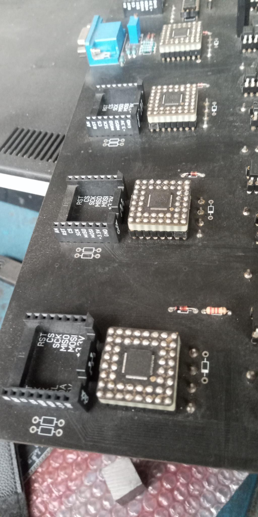 Edited 2026-05-08 02:36 by PhenixRising |
||||
| Mixtel90 Guru Joined: 05/10/2019 Location: United KingdomPosts: 8938 |
No, that's not easy. I found the best way was to do the following: When fitting: Start by plugging the male and female connectors together Hold the module in position by soldering a pin on each side Turn the board over and solder all the pins Turn it upright again and solder the remaining top pins. The male and female pins are now aligned precisely, making fittind and removal a bit easier. When removing: Ease each side up slightly using a thin bladed screwdriver I then have a wider, still thin bladed, screwdriver that I can use to ease the module out. Mick Zilog Inside! nascom.info for Nascom & Gemini Preliminary MMBasic docs & my PCB designs |
||||
| matherp Guru Joined: 11/12/2012 Location: United KingdomPosts: 11604 |
Lyle, there is a bug in the A axis I'm working on. So don't waste time on it. |
||||
| Bryan1 Guru Joined: 22/02/2006 Location: AustraliaPosts: 2136 |
Morning Guy's, Well as it has been a couple of years since I used Sprint Layout it was fun yesterday and now I feel I do have that bug and the grey cells are starting to come back so this first draft is just the start. Off memory with a double sided board I do need to put via's in and reading the pico manual yesterday a sckotty diode to Vbus can be used for the power input. Now with the I2C lines as I'm famous for getting it wrong SDA on the RTC does go to the SDA on the pico right ? With my design for this project the LCD won't be connected to the PCB and it will be put in a small case and mounted in a suitable place for easy viewing. Also with the first draft I almost got it all single sided so my goal today is to try and keep it single sided then I could even just mill the board on my CNC. Anyway the first caffine hasn't hit the sides so more thinking and pondering to do.Lyle thanks for the offer of one of those silly chip boards but my motto has always been if I want something just make it myself and in these later years if it can go wrong it will go wrong Just look at my inverter project for an example anyway yesterday I did see that inverter hit 50Kw/hour When all the lights are turned off the it sits on 5-6 watts and with those 3 off 330 watts panels leaning on the side of my shed the shed battery SG is rarely below 1240 Later today after I have another play in Sprint Layout I will zip up the file and post it on here so all the Sprint Layout guru's can have a good laugh at my efforts Regards Bryan |
||||
| Bryan1 Guru Joined: 22/02/2006 Location: AustraliaPosts: 2136 |
Ok Guy's managed to get the PCB all single sided with only 2 links.pico 2 board.zip 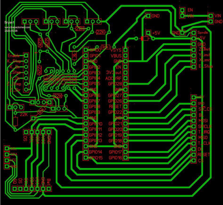 Now I have some 5V and 3V3 breadboard friendly power boards so thats what in the top corner, now I just use a pair of lithium batteries and I do have some lithium chargers so when the battery gets low I can charge it. Now it is a shame we used all the analogue inputs as the battery voltage shown on the lcd. Now this may be a hair brain idea as I could use a 2040 zero to look after the battery and set it up for I2C so the battery voltage can be displayed on the LCD. Anyway time for a caffine so guy's have fun tearing down my effort as I'm sure it won't make guru standard Now doing the DRC all the pads on the IC and sip connectors are saying drilling too close so not sure why. Regards Bryan Edit: Second take this morning so added +5V and GND to the LCD sip and put in a 4 pin header for SDA and SCL so the zero can be added. Also just updated again as I added +5V and GND for the zero power. Edited 2026-05-08 11:53 by Bryan1 |
||||
| Bryan1 Guru Joined: 22/02/2006 Location: AustraliaPosts: 2136 |
Ok finally got the DRC down to the 45 degree link, I did try deleting the 10mm resistor and even redid each pad by doing a paste of the pad that did clear DRC. Now no matter what I've tried hasn't worked so Mixtel can you please fix this for me then the PCB will pass the DRC. Also I redid the macros so it passed DRC where before I didn't do a DRC  pico 2 board.zip Here is a pic with the ground plane in 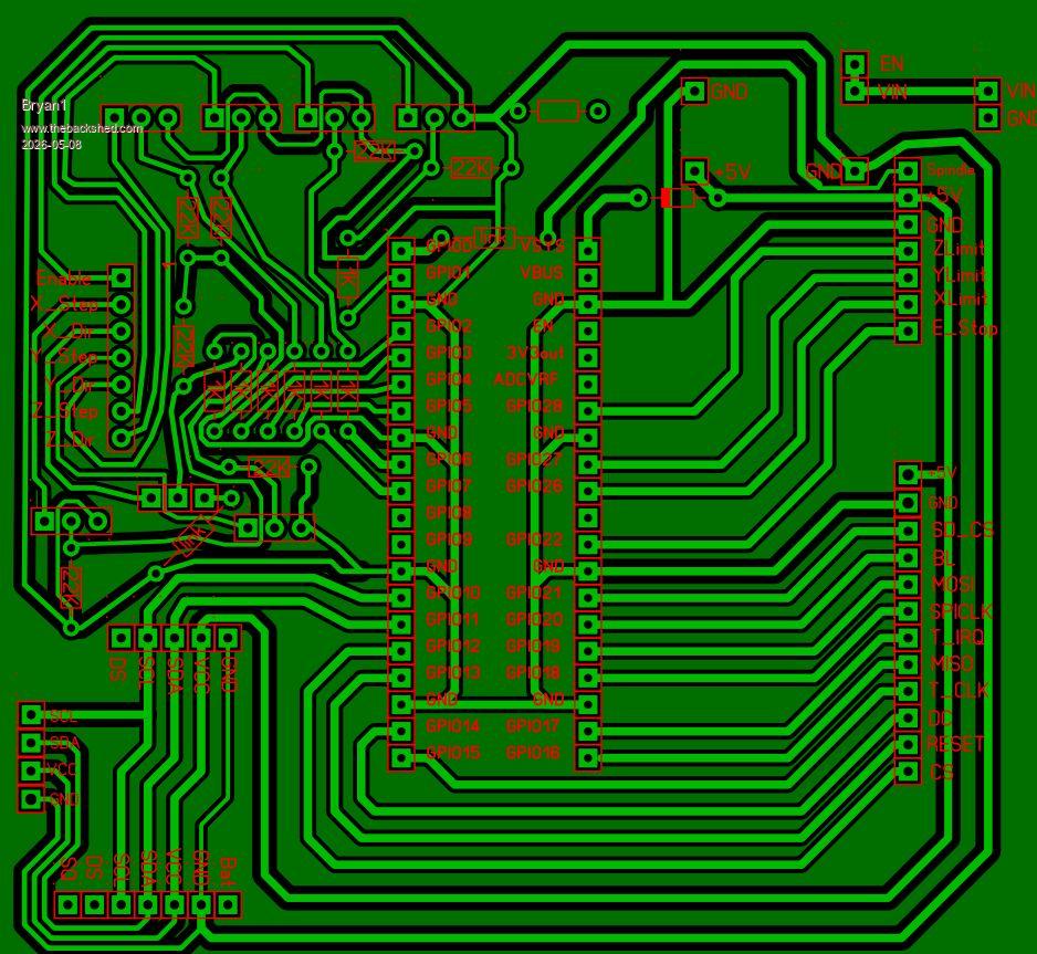 Regards Bryan Edit: I found removing the SIP pads for the link cured the DRC now strangely just about every other connection is the same. Edited 2026-05-08 14:04 by Bryan1 |
||||
| Volhout Guru Joined: 05/03/2018 Location: NetherlandsPosts: 5975 |
Hi Bryan, 1/ The ground plane looks not connected. Maybe you should connect it to GND to get best performance. 2/ Maybe this is the graphics... but it looks as if there is solder mask on the pads. Please check this out before ordering. Otherwise you cannot solder anything to the board. Volhout PicomiteVGA PETSCII ROBOTS |
||||
| Bryan1 Guru Joined: 22/02/2006 Location: AustraliaPosts: 2136 |
Ok just worked how to do the thermal pads so this means a total new design for the pcb and solve the problem of GND ? |
||||
| BarryH Regular Member Joined: 05/01/2025 Location: AustraliaPosts: 47 |
Hi Bryan, - the 4 pin I2C pins on the bottom LHS are not interspersed correctly (not 100 mil distance between them). The minor distance issue may not have a real world effect. - the top 2 pads of the 12 pin display connector on the RHS are not interspersed correctly. The minor distance issue may not have a real world effect. Now that you have re-caught the bug for Sprint Layout, there is an excellent free plug-in called sprintFont available from https://github.com/cdhigh/sprintFontRelease which provides Teardrops to pads, Rounds tracks, and a few other great features. cheers Edited 2026-05-08 17:45 by BarryH BarryH |
||||
| Mixtel90 Guru Joined: 05/10/2019 Location: United KingdomPosts: 8938 |
It's usual to use thermal pads and the ground plane as your common GND connection everywhere. It's also important that you use the test pen to make sure that you do a point-to-point check on everything. If you've been messing about you can sometimes get traces that don't quite reach a pad or isolated thermal pads that aren't actually connected to GND because other traces are in the way. If you click on the red Solder mask button all masked areas light up. If you click one of these it goes out and mask is applied. This is very handy with vias as you want them masked even though they are actually through pads. Unfortunately SL6 has no built-in concept of vias. I changed the colour scheme, but that's up to you. Something I learned on the CAD at work is that red is a dark colour and not easily seen on a black background. You can have several user-defined schemes if you like. :) Options/General Settings/Colours If you are using 1A Schottky diodes then be aware that their leads are quite thick (like a 1N4007). I usually use 1mm for them. BE AWARE! JLCPCB don't do single sided boards and every hole is through-plated by default. So, if you use them, treat it as a double sided board. Mick Zilog Inside! nascom.info for Nascom & Gemini Preliminary MMBasic docs & my PCB designs |
||||
| Bryan1 Guru Joined: 22/02/2006 Location: AustraliaPosts: 2136 |
Ok finally got there and found I had to put a ground plane on C1 layer in oder to get 3 transistor emitters to attach to ground. I did find doing a via on the LCD SIP did the trick pico 2 board.zip 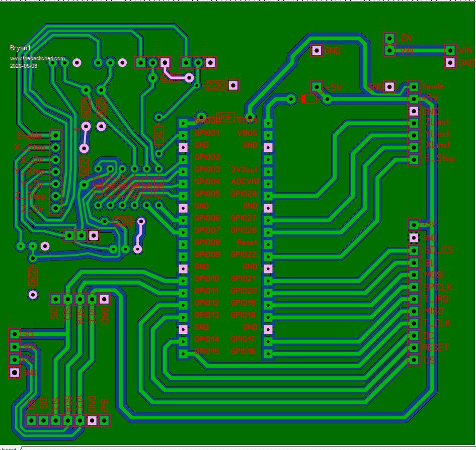 Now I do have some double sided PCB boards here but as it's only a 100x100 board getting them made at JLCPCB may be the go. Regards Bryan Edit : didn't see the posts as I was typing OK so make the gaps on the traces wider apart so they are more than 100 mil apart, now for the scotty diode as I have some off my inverter project I was just going to use one of them Edited 2026-05-08 18:22 by Bryan1 |
||||
| Bryan1 Guru Joined: 22/02/2006 Location: AustraliaPosts: 2136 |
OK went and did a DRC and found a few errors so fixed them all so got the all clear there. So if the design committee is happy then it's ready to go to JLCPCB to get the boards made. 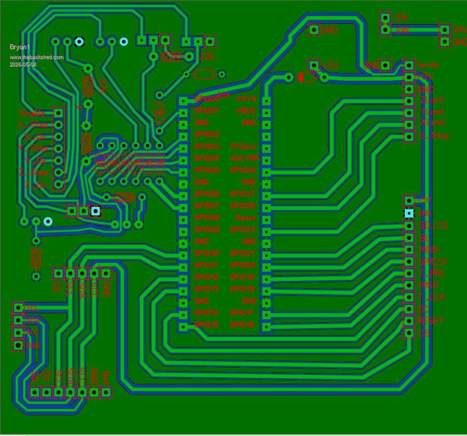 pico 2 board.zip Regards Bryan Edited 2026-05-08 18:52 by Bryan1 |
||||
| Mixtel90 Guru Joined: 05/10/2019 Location: United KingdomPosts: 8938 |
Something else to watch is hole diameters. Generally male pin headers need 0.9mm or 1mm, female sockets can be as small as o.77mm or 0.8mm. It looks like you maay have done something like this already. When I have thermal pads in the middle of a row I usually turn off the connections facing the adjacent pins. It's not strictly necessary unless you are running a trace between them, but I do it anyway. :) You've got the VSYS and VBUS pins swapped, haven't you? There is an on-board diode from VBUS to VSYS on a Pico so you can power it directly into VSYS without a back-feed to the USB socket (VBUS). You may want a diode from the external circuit to VSYS so that it doesn't get powered when you are updating firmware over USB. It's purely optional usually. Mick Zilog Inside! nascom.info for Nascom & Gemini Preliminary MMBasic docs & my PCB designs |
||||
| The Back Shed's forum code is written, and hosted, in Australia. | © JAQ Software 2026 |
