
|
|
Forum Index : Electronics : Various aspects of home brew inverters
| Author | Message | ||||
| johnmc Senior Member Joined: 21/01/2011 Location: AustraliaPosts: 283 |
Most impressive poida, and many thanks for the pictures and your effort, this helps me understand the concept, of how you are synchronising the two ac inputs, with your code. cheers john johnmc |
||||
renewableMark Guru Joined: 09/12/2017 Location: AustraliaPosts: 1679 |
I ordered some nano boards, have 4 spare if anyone wants one. $10 plus post. 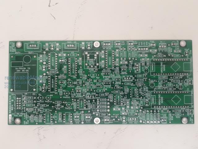 Cheers Caveman Mark Off grid eastern Melb |
||||
| johnmc Senior Member Joined: 21/01/2011 Location: AustraliaPosts: 283 |
Good day Mark, I will take two boards . cheers john johnmc |
||||
| renewableMark Guru Joined: 09/12/2017 Location: AustraliaPosts: 1679 |
ok 2 left Will send pm John. Cheers Caveman Mark Off grid eastern Melb |
||||
| Mulver Senior Member Joined: 27/02/2017 Location: AustraliaPosts: 160 |
I�ll have one if that�s okay! Cheers Shane |
||||
| renewableMark Guru Joined: 09/12/2017 Location: AustraliaPosts: 1679 |
Edit, All gone. Cheers Caveman Mark Off grid eastern Melb |
||||
| wiseguy Guru Joined: 21/06/2018 Location: AustraliaPosts: 1297 |
Hi TinyT, I am implementing my version of a control board bit by bit and I hit a small stumbling block. I refer to your schematics to ensure I have the right pin numbers etc. Nano1 has an input shown as "SCR_SD_N" which caused me to re read about 40 pages to discover what the hell it was. After looking at Nano2 which also has this mysterious input I think I now get it. Does Nano1 have the flag the wrong way around - it is an output to nano2 so Nano2 knows why the toroid has suddenly gone so quiet, and why the lights went out.... I'm glad to see the finished results are starting to make some sine waves. I only have 2 types of outputs from my control board to the power boards as I will only be driving optos. One uses the IR2184 direct to optos in the standard fashion (with inherent dead time), the second type uses a quad exclusive or gate to provide complimentary drives (no dead time) which are intended to drive the opto couplers using Warps inverse parallel trick and can provide for more (increased) dead time by adding a small cap if required. Hope to send out for manufacture this week. If at first you dont succeed, I suggest you avoid sky diving.... Cheers Mike |
||||
| nickskethisniks Guru Joined: 17/10/2017 Location: BelgiumPosts: 481 |
Hi wiseguy, make sure you your opto's can be driven in reverse! |
||||
| tinyt Guru Joined: 12/11/2017 Location: United StatesPosts: 561 |
The way I remember, signal SCR_SD_N is input to nano1 and nano2. It is output from the SCR (Q6) thru a 1K resistor (r27). It becomes high when the SCR conducts. It now depends on poida's codes how nano1 and nano2 handles it. |
||||
| wiseguy Guru Joined: 21/06/2018 Location: AustraliaPosts: 1297 |
Thanks Nick I suddenly got worried - some optos uses a pseudo diode (electronic coupling using inductors or capacitors) for bridging signals across the isolation barrier and these may not like reverse potential. I re-checked the data sheet for the TLP152 I will use, it is a standard type opto with a reverse capability of 5V so it is OK. Hi TinyT - your memory is fully functional.... I looked at that schematic many times I saw the SCR_SD but missed the flag just under it to the right of R27 - thank you! If at first you dont succeed, I suggest you avoid sky diving.... Cheers Mike |
||||
| poida Guru Joined: 02/02/2017 Location: AustraliaPosts: 1480 |
Part 26: A closer look at MOSFET gate voltages during switching In another post on this forum, some interest in shoot through or cross conduction as a failure mode has been shown. For this discussion, I want to look at one of the 2 half bridges of the MOSFET switched output stage of the inverter. There is no need to examine both of the half bridges, what we see in one of them is reproduced in the other. Shoot through is defined to be when both the high side and low side MOSFETS conduct at the same time. This is obviously a bad thing, it means the DC supply is conducted through both sides of the half bridge, effectively shorting the DC supply, with current limited by the Rds(on) resistance and DC supply impedance. Some inverters have immense DC supply capacitance and this provides a huge potential current during short circuits. Reading the specifications of MOSFETS used in these applications, we see something called Vgs(th) which is the gate voltage, with respect to the Source pin, that is needed for the MOSFET to show clear signs it is conducting. Not completely conducting, at it's specified Rds(on) resistance, but conducting never the less. The testing and results that follow are using my test inverter, which uses IRF3808. I have 4 MOSFETS for each of the 4 legs of the full bridge. Each leg is fed gate drive that is connected to 4 MOSFETS in parallel. This is not best practice and risks having one of the 4 switching on a little before the others, and this can be a cause of catastrophic failures. It very probably causes some high frequency oscillation. The IRF 3800 Vgs(th) is between 2V and 4V Rds(on) is 5.8 mOhm Pulsed current max is 550 A, continuous curent is 140A at 25 degC at the junction. These are reasonable devices for a test inverter. I want to show the gate voltages (with respect to the low and high side's Source pin) with the half bridge output voltage. This voltage is measured at the point where we connect the primary winding of the output transformer. Yellow is low side gate voltage Dark Blue is high side gate voltage (with respect to high side Source pin) Light Blue is the output voltage of the half bridge It appears I am using only about 10V to switch the gates. It's clear also the DC supply of the inverter is about 30V as seen in the light Blue amplitude. First an overview. To make sense of this, see the upper trace, this shows a bit more than one complete 50Hz output. I am running the current nanoverter code, so it shows clearly the activity of one of the half bridges. There is a small vertical dark line on the left in the upper trace. This shows where in time the time expanded bottom view is taken from. 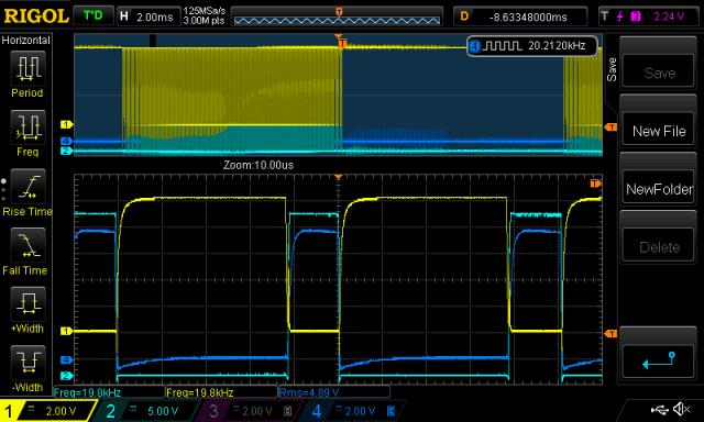 Now let's see the low side switch ON event. We will see the following: the high side gate go low, with a bit of dead time to allow the... low side gate go high. Output voltage drop to zero as the lowside MOSFETS conduct, pulling the output to ground 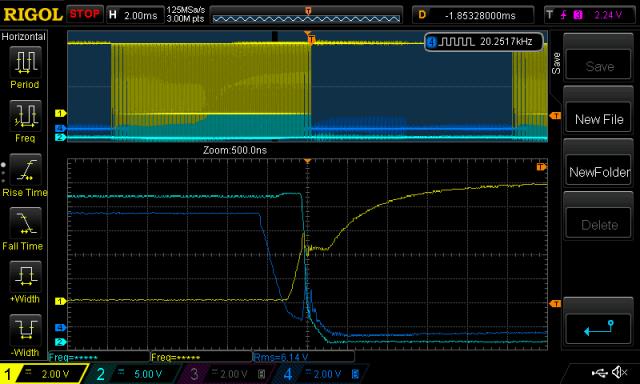 And what else can we see? The high side gate voltage increase, way past the Vgs(th) during the rapid drop of the output voltage. You can see it, right in the middle of the lower trace. When I look at the original image I see it peak over 6V. This is likely resulting in some low power shoot through. A detail to see, but most importantly, is to observe the low side gate starts to rise on a slope (defined by gate drive current, gate supply resistance and gate capacitance) until the MOSFET finally conducts fully. This slams the output voltage down to ground rapidly. This fast voltage change, which appears on the high side source pin, as well as the low side drain pin causes the high side gate voltage to rise. Well past threshold voltage. Into conduction. Beyond our control. I show now the low side switch OFF event. 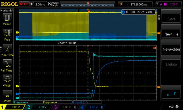 This is showing what we all think is supposed to happen. We still see some dv/dt induced gate voltage changes. As the output voltage rises rapidly, it causes the high side gate to drop a little, below zero in fact, for a short time. Looking at the switching at a different time in the 50Hz cycle, we can see some ugly high frequency oscillations, and shoot through. 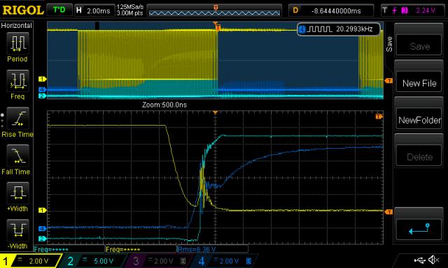 As the low side gate is driven low, the dead time permits us to see for a short time no output voltage, low voltage on both the high side and low side MOSFET gates. Then it's time to drive the high side MOSFETs ON, pulling the output voltage HIGH. And all hell breaks loose. As soon as the output voltage rises quickly, the lowside gate is now rising well past threshold and conducts. I want to make it very clear: The low side gate is no longer under control of the gate drive IC's output. It is being pulled low by the drive IC, via a 4.7R resistor but voltages arising within the low side MOSFET is causing their gates to rise up well past threshold values. These gate voltages also appear on the drive IC output pins, to a certain extent as well. This is another issue to explore. This clearly is not a smooth event, the low side gate is oscillating up and down, pulling the output voltage every which way and causing further dv/dt induced changes. I have attached a current sensor to the DC supply in the past and clear spikes in DC supply current occur during these frenzied switching events from the shoot through. Notice the output voltage only rises after the high side gate has been charged up enough, into it's fully enhanced conduction stage. These captures are really very nice, and show the gate voltages just as illustrated in the textbooks (and other publications) Finally, we see the high side switch OFF event, at this location in the output waveform. Again we can see more dv/dt induced gate voltage change. The high side gate is pulled low, first a pause as we discharge the capacitor present on the gate, in the chips, then it drops to a value to permit the conduction to stop. 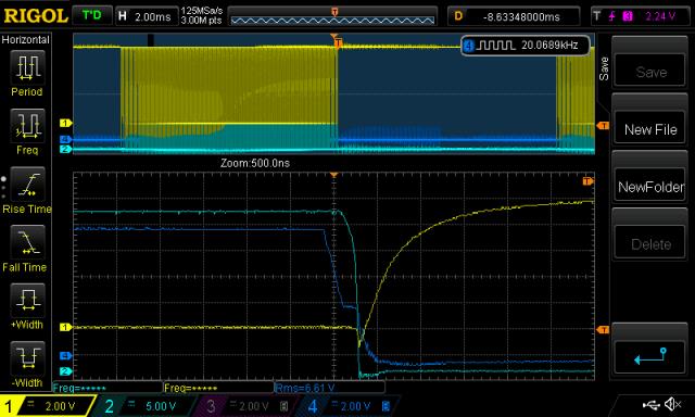 I want to explore further gate voltage behavior in SPWM inverters. I have one of Madness's power boards, which use beefy transistor based totem pole drives for both low and high side gates. I suspect this approach (totem pole drive) will give a much lower impedence drive to the gates, potentially reducing shoot through. It will almost certainly isolate the gate drive IC output stages from undesirable dv/dt induced voltages coming from the MOSFET gates. The IR2110 has specifications that clearly state that we must never let their outputs go below -0.3V compared with ground(low side Source voltage) or VS (the high side Source voltage). I fit TVS protection to my inverters, protecting the drive IC outputs ONLY. With a totem pole drive, maybe we will get 2, much needed benefits. I need to find the time to build Mad's board and then we can find out. A deep understanding of these switching events is needed, in my view, for us all to make continued progress in our building and use of home made inverters. wronger than a phone book full of wrong phone numbers |
||||
| wiseguy Guru Joined: 21/06/2018 Location: AustraliaPosts: 1297 |
A great presentation and informative analysis of FET switching behaviour. In my experience individual chokes in series with each of the paralleled FET gates in the form of a ferrite bead or 5-10uH choke often helps quench HF oscillations - these can be in the MHz range. In the second to last CRO picture, the yellow gate display appears to show that the gate was not fully off when it reversed direction into the oscillation area. If I am reading the CRO correctly the fall of the gate transition is ~ 500nS, relatively slow. A parallel diode across the gate resistors (cathode facing away from the gate) should help speed up the fall time, a 1N4148 may be sufficient but I usually use a power ultrafast diode such as MUR160 or UF1004. A lower value resistor may also help. - but these both create a higher drive requirement of the Gate drive IC or buffer used. I have found that the slower the change of gate voltage is as it passes through the miller region can make it more prone to oscillation issues. When there is a fast transient on the Drain, it is coupled back to the Gate. The Gate resistor forms a differentiator with the Drain - Gate capacitor and a combination of fast transient and insufficiently low Gate impedance (series r - even with the driver output low as you found)) can definitely drive the gate sufficiently to cause the FET to begin unintended conduction. If at first you dont succeed, I suggest you avoid sky diving.... Cheers Mike |
||||
| poida Guru Joined: 02/02/2017 Location: AustraliaPosts: 1480 |
For sure these little beads can do wonders. I trialed one bead only once and saw the rise time of the gate voltage become way too slow. no numbers, sorry, it's from the dim dark corners of the memory. But certainly, if I took the time to specify and source reasonable value ferrite beads I think we could remove some of the circus of oscillations wronger than a phone book full of wrong phone numbers |
||||
| poida Guru Joined: 02/02/2017 Location: AustraliaPosts: 1480 |
all four legs of the full bridge have diodes as you suggest. I'm pleased somebody say this anomaly. I have no idea why it is so. Maybe I've blown the diode in question. They usually die short tho. I would love to start driving these gates with some serious low impedance drive. It would be a detail design thing: thick conductors everywhere short conductors too low gate resistors the diodes you mention all driven by a beefy drive IC or totem pole or special opto coupler, whatever tickles yer fancy. I want to be able to sink that dv/dt, or maybe dI/dt parasitic down to local Source level via almost zero resistance. That would be nice. wronger than a phone book full of wrong phone numbers |
||||
| poida Guru Joined: 02/02/2017 Location: AustraliaPosts: 1480 |
As you say, it can happen and I showed it happening in the above post. I think I see this as theory looking to start a fight with us and we better be ready. wronger than a phone book full of wrong phone numbers |
||||
mackoffgrid Guru Joined: 13/03/2017 Location: AustraliaPosts: 460 |
Poida Great post mate. Amazing timing - I've been working on dvdt this week. What I have found is that dvdt can cause minor shoot-through at quite slow changes in Vdrain (and less so Vsource). Much slower that the data sheets suggest. I have included in my driver board a clamping FET which directly clamps the Gate (200 mOhm) to ground and it will still experience some turn-on, via Cgd. I can reduce the shoot-through, say of the lower fet, by slowing down the turn on action of the upper fet, particularly until Vthreshold. I did this by adding an inductor in series with Rg, which I also increased in value. You could also do this by adding more inductance to the load. I am very jealous of your CRO, and diff probes. Which diff probe are you using?. I am about to try a different drive circuit where I clamp the gate to -5 or -12 volts. The reason I'm doing this is that it will take a lot more charge from Cgd before Cgs charges up to its threshold voltage. I believe it is important to get this right at no load, because High loads are likely to be inductive and will slow dvdt, its at no load that dvdt will show it affects and possibly will cause destruction of the mosfets. Cheers Andrew |
||||
| mackoffgrid Guru Joined: 13/03/2017 Location: AustraliaPosts: 460 |
To expand what I found with dvdt, and shoot-through. BTW, this dvdt, parasitic effects are more prominent in large fets. I believe the ideal approach was to slow down the initial Gate drive current until Vgs has reached the miller plateau, by which time Vdrain-source has aceived a lot of its transition, then speed up the drive current so as to achieve low Rds. Slowing down the transition solves the dvdt problem but when multiple parallel mosfets are involved we are possibly getting into Spirito Effect territory, forward biased, linear region driving large currents. Cheers Andrew |
||||
| poida Guru Joined: 02/02/2017 Location: AustraliaPosts: 1480 |
one of these I bought it via ebay years ago. It's good for reasonably low level stuff as well as mains type voltages. wronger than a phone book full of wrong phone numbers |
||||
| poida Guru Joined: 02/02/2017 Location: AustraliaPosts: 1480 |
Yes, biasing the gate drive to -5 or so volts is the best way to go. We need a drive that has a low output of -5V and a high output of +15 all with respect to the FET's Source pin. That will reduce to nearly zero the shoot through. How to do it... Some designs I've seen use pulse transformers with a DC negative bias applied to the output. Others don't use the pulse transformers at all. wronger than a phone book full of wrong phone numbers |
||||
| poida Guru Joined: 02/02/2017 Location: AustraliaPosts: 1480 |
I agree that no or low load conditions are frequently present when an inverter fails. My blowups all were at 500W sort of loads, where the board can do 2.5kW and everything else is good for those sorts of power. My view at the moment, and I am prepared to change it when I see things that demand a change, is that the MOSFET bridges we build can easily take the sorts of power we put through them. Even when there is likely some shoot through. My view is that failures of mine are due to the dv/dt induced gate voltages can some times be fed back into the gate drive IC output stages where they must never reach less than -0.3V to ground (low side) or -0.3 to VS (high side) When this happens the totem pole FET output stage in the IC can blow, likely shorting to high. If it fails, shorting to low, the MOSFET bridge will have one leg never switched ON and so no problems. wronger than a phone book full of wrong phone numbers |
||||
| The Back Shed's forum code is written, and hosted, in Australia. | © JAQ Software 2026 |
