
|
|
Forum Index : Microcontroller and PC projects : MOSFET question....
| Author | Message | ||||
Grogster Admin Group Joined: 31/12/2012 Location: New ZealandPosts: 9975 |
In my attempt to teach myself how to use MOSFET's over BiPolar transistors, I thought I would have a go at a simple battery trickle-charging circuit. The following image show the existing arrangement I have on the left, and the proposed on the right. I was wanting to add a transistor to turn off the charging if it was left on the charger for more then 12 hours. That's the idea, anyway. 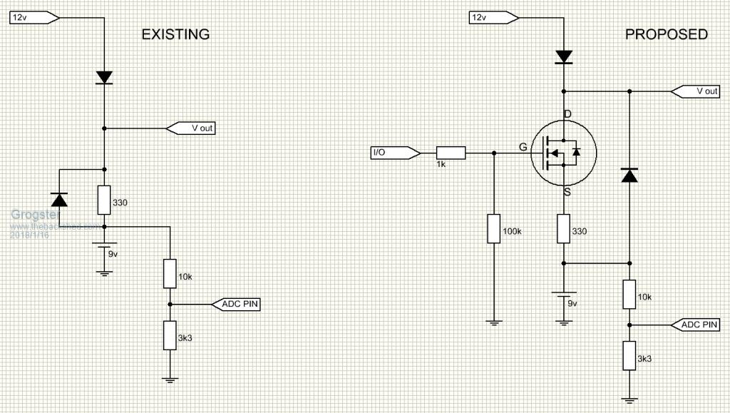 The one on the left works fine, but there is no control over it - it is forever on trickle-charge, which will shorten the battery life a little I guess. The on the right is what I want to do, and the MOSFET would be switched on by the MCU when the charger is plugged in. If after about 12 hours, the charger is still plugged in, it will disable charging any further by setting the MOSFET I/O line low, and stop blinking the charging LED. Transistor should then switch off, preventing any further charging. Diode-gate on both schematics allows for either the battery or the external supply to keep the MCU running. Not shown here is the 3v3 regulator and associated MM2 parts, but the 3v3 regulator is fed from the diode-gate. I am hoping that what will happen will be that the MOSFET will turn on during initial plug-in of the charger, allowing a trickle-charge current to flow to the battery. When times up, if charger still plugged in, MOSFET will switch off, stopping the battery charging anymore. If charger is removed, the diode gate will bypass the MOSFET and charging resistor, and power the circuit. As I am not terribly familiar with MOSFET stuff, and am trying to teach myself something about using them, I expect this circuit might be wrong, so I would like to ask the members more in the know then me here. I fully expect redrok to chime in with a plethora of mathematics....  An ADC pin also measures the battery voltage when the charger is removed, and this could also be used in the charging routine if I have the MOSFET bit right. IE: Charge for 12 hours or so, turn off MOSFET, read ADC battery voltage. If still low, keep charging. If OK, stop charging - that kind of idea. EDIT: Oh, there is also a 10k/3k3 potential divider on the DC input, which is connected to another MM2 pin as a 'DC-DETECT' line. If this goes high, the MM2 knows the charger has been plugged in, so goes to the charging routines, and stops the main routine that runs when the charger is removed. Smoke makes things work. When the smoke gets out, it stops! |
||||
TassyJim Guru Joined: 07/08/2011 Location: AustraliaPosts: 6538 |
You will need two transistors/mosfets to switch on the high side. 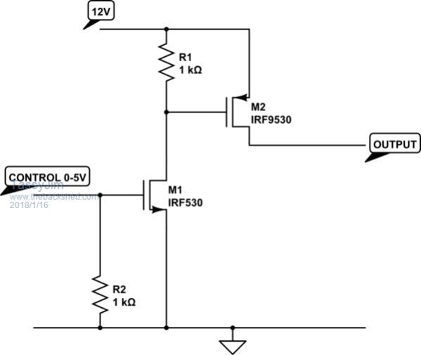 This is the first circuit I found with google that gives the idea. Adapting it to your needs is straight forward. Jim VK7JH MMedit |
||||
| Grogster Admin Group Joined: 31/12/2012 Location: New ZealandPosts: 9975 |
Why? With an N-channel MOSFET, you should be able to drive it directly with the MM2 I/O pin.  If a P-Channel MOSFET, I have needed the extra NPN transistor on the MOSFET gate. Or is it simply cos the Source of the MOSFET in this arrangement is higher then ground, so you still need the helper transistor? IE: When using as a LOW-SIDE switch, you don't need any extra 'Help', but if it is high-side, you do. EDIT: Oh, do you mean change the MOSFET to P-channel and use a helper transistor like this: 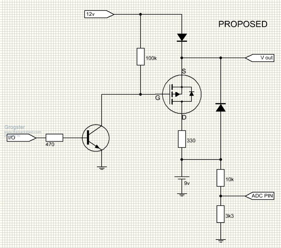 Smoke makes things work. When the smoke gets out, it stops! |
||||
Azure Guru Joined: 09/11/2017 Location: AustraliaPosts: 446 |
Yes, you'll definitely need a level translator to drive a high side switching mosfet from a digital level control signal. It needs to be driven to a level relative to the source voltage and devices Vgsth. |
||||
| Solar Mike Guru Joined: 08/02/2015 Location: New ZealandPosts: 1213 |
You are on the right track Grogster. Suggest change the 100k on the gate of PChan to between 2 to 10k, add a 10k base to gnd of the driver npn, so when your cpu first starts up its io pins are normally floating until initialized by code, and the driver may turn on and cause issues with high impedance input. If your 12v supply has any possibility of voltage spikes the gate of the mosfet may be exposed and would blow up, placing a 12 volt zener gate to source will stop that possibility. Cheers Mike |
||||
| The Back Shed's forum code is written, and hosted, in Australia. | © JAQ Software 2026 |
